The expansion of GaN applications, like in other semiconductor technologies, will require a range of options forpatterning and etching. Since GaN strongly resists wetetches1, more complex and expensive processes have beenrequired, primarily those using reactive ion etching ~RIE!.2,3Here we report good results obtained by structuring with ahigh-energy pulsed laser, removing 10–70 nm of materialper 5 ns pulse. This compares very favorably in speed andprofile quality to the RIE, where rates of 50 nm/min are verygood.3 The dominant physical mechanism for the etching isidentified as thermal decomposition with resulting nitrogeneffusion. Because the heat is generated in a short time, veryhigh spatial resolution is possible, as demonstrated here using interference gratings. Residual gallium can be removedchemically. This mechanism also appears responsible for asimilar etching process recently reported,4 where pulsedlaser exposure was performed in a HCl ambient. Our resultsshow that the strong illumination and the chemical etchantact separately. This differs from another recent work wherewet etching of GaN is enhanced using a continuous laserbeam, apparently by a photoelectrochemical process.
The GaN films were grown on sapphire ~c-Al2O3) substrates both by metal-organic chemical vapor deposition~MOCVD! and molecular beam epitaxy ~MBE!. They wereabout 1 mm thick, and of good epitaxial quality as describedelsewhere.6,7 The MOCVD samples were grown at 950 °Cusing triethylgallium and ammonia. The MBE films weregrown at a rate of 0.4 mm/h at 900 °C, using a rf-plasmanitrogen source. Characterization of the films determinedhelium-temperature photoluminescence at 3.467 eV with5–10 meV halfwidth, and x-ray diffraction rocking curveswith 300 arcsec halfwidth.
Structuring was done with the 355 nm ~3.5 eV!, thirdharmonic of a Nd:YAG pulsed laser. The pulse duration isnominally 5 ns and the beam diameter is about 7 mm. Pulseenergies were 50–200 mJ, yielding 130–520 mJ/cm2. In order to determine resolution and to test a promising patterningmethod, a grating was produced by splitting the pulse beamand bringing the two beams together on the sample to makea striped interference pattern. The setup was only recentlydescribed.
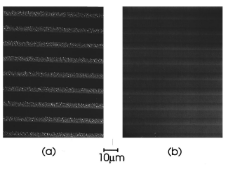
Figure 1 shows optical micrographs of a film that was structured in air with a single 100 mJ pulse ~corresponding to420 mJ/cm2 peak intensity estimated below!, with the twobeams at near-normal incidence, producing a grating periodof about 11 mm. After the pulse, the normally transparentfilm was noticably darkened to the eye, apparently by Garich material. In Fig. 1a, lightly contrasting trenches withsharp edges are visible; they contain what appears to bedroplets of gallium. This was confirmed by dipping thesample in HCl for a few seconds, which quickly removes Gametal but leaves GaN undamaged. The result is shown Fig.1b, where clean trenches with somewhat better contrast areobserved. After the HCl etch, the film was again transparentand showed diffraction from the etched grating. Further support for the decomposition explanation was obtained whilestructuring samples immersed in liquid ~HCl solution!, asdescribed below, where bubbles were observed rising fromthe sample immediately after the pulses. These are probablymostly nitrogen, since any water vapor produced at the surface should quickly condense in the cooler temperature liquid.

Fig1
Topographic measurements, using an atomic force microscope ~AFM!, reveal the shape of the trenches, as shownin Fig. 2. With 100 mJ and a 6 mm grating, the trench widthsare half the grating period, and the depth is near 70 nm. Thesharp edges and flat mesas are particularly attractive. They as deeply per pulse. This would be the case for the 193 nmexposure reported in Ref. 4, for which the penetration depthis about four times shorter, as estimated from values in Ref.10. Since the etching was performed differently however,and over many pulses, the etch rate is not able to be directlycompared.