Indium phosphide is the material of choice for monolithic integration of optical components. This material system is suitable for application in optical communication. Photonic Integrated Circuits (PICs) on InP create the possibility for mass production to fulfill the increasing demand for more complex optical functionality at ever-lower prices.
The basic building block for PICs is the optical waveguide. Usually this is a ridge etched in a layer stack on an InP-substrate. Various etching techniques have been developed over the years. Reactive Ion Etching (RIE, [1]) has emerged as the most flexible and effective technique to obtain these waveguides. One specific problem associated with RIE is surface damage caused by impact of ions and by the chemical process. Various adjustments to RIE have been proposed and developed to reduce this problem. Electron Cyclotron Resonance (ECR) is expected to result in lower impact damage, because the plasma is ignited in the ECR column away from the sample, which is placed on the lower electrode in the chamber. We have developed an ECR-process for waveguides on InP [2]. In order to examine the loss mechanism we also realized wet-chemically etched waveguides. These have no surface damage, but are more sensitive to the sidewall roughness because of their different shape.
The waveguide is designed to provide monomodal propagation for both the TE and the TM polarization. This requirement limits the thickness of the waveguiding layer, the width of the ridges and the etching depth. The layer stack (see fig.1) is grown on an undoped InP-substrate and consists of two also undoped layers. The waveguiding layer, with a thickness of 600 nm, is an InGaAsP-layer with a bandgap of 0.956 eV, corresponding to a vacuum wavelength of 1.3 µm. The top layer of InP is 300 nm thick. Simulations with a vectorial waveguide solver [3] showed that waveguides as narrow as 1.5 µm would be multimodal for TM if the ridge is etched 100 nm into the quaternary layer. To avoid this the etching depth was limited to the thickness of the top layer: 300 nm. This results in a strip-loaded waveguide. The selective wet chemical etch will also provide this depth, making comparison of dry- and wet-chemical etched waveguides poss.
For dry etching, we use a microwave (2.45GHz) Electron Cyclotron Resonance (ECR) sourceand CH/H,/Ar discharges with additional radio frequency (13.56MH2), resulting in aseparately addressed DC bias. Smooth surface, reasonable (-20 nm/min) etch rate and verticalside-walls have been achieved. The process conditions are as follow: CH:H,Ar / 10:18:8 sccmat 150 W with a DC bias of-200V. Higher power would result in higher etch rate but roughersurface. Photoluminescence (PL) measurements on etched samples have shown a PL-intensityreduction. The reference level was recovered however after a short O, plasma treatmentfollowed by a dip in 10% HCl. Schottky diodes were made on p-InP substrates after ECRetching and characterised. The barrier height and the ideality factor were fully recovered afterthe O, plasma treatment and the dip in 10% HCl. The wet-etched waveguides are realizedthrough InP-selective wet chemical etch with a suitable etchant (C;H;O;: HCl: HCIO4 , 57). Inthis way a ridge is obtained with sidewalls at angles of 35 degrees with the chip surface.
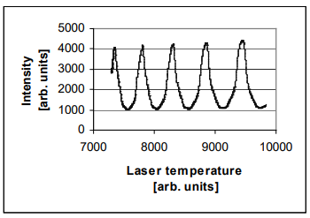
Prior to ECR etching, the protective top quaternary layer of 5 nm was removed using a selectivewet etching. Subsequently etching of the waveguides was performed using the ECR dry etchingprocess and the wet-chemical proces described above. Cleaving the sample into bars withvarious lengths formed the mirrors necessary for the Fabry-Perot loss measurements of thewaveguides. Figures 2 and 3 show SEM photographs of dry etched and a wet etchedwaveguides. The SiNx masking pattern is still visible on top of the waveguides.

Fig1
The ECR-etched and the wet-chemically etched waveguides are made from the same wafer, andtherefore causes 3 and 4 do not lead to differences between them. This does not hold for theirst two causes mentioned. A dry-etching process will involve some physical sputteringbecause of the ions colliding with the surface. Furthermore, a phosphorus-depleted layer caneasily occur, since the gaseous P-containing reaction products of the etching process are themost volatile. Removal of this layer with an HCL-dip results in extra roughness of the etchedsurfaces (see fig.2). For wet-chemical etching this type of damage does not occur, since there isno ion impact and there are no volatile reaction products. On the other hand, the influence ofthe sidewall roughness is much larger for the wet-etched ridges. Because of the different shape(angled sides) of the etched ridges the sidewall area is larger than for the dry-etched samples, sothat the scattering for the guided modes due to the sidewall roughness is stronger.
下一篇: III-V Si 光子通过芯片到晶圆键合