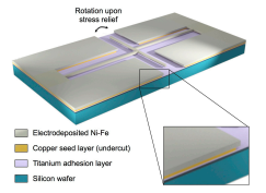
This article presents a set of low-temperature deposition and etching processes for the integration of electrochemically deposited Ni-Fe alloys in complex magnetic microelectromechanical systems, as Ni-Fe is known to suffer from detrimental stress development when subjected to excessive thermal loads. A selective etch process is reported which enables the copper seed layer used for electrodeposition to be removed while preserving the integrity of Ni-Fe. In addition, a low temperature deposition and surface micromachining process is presented in which silicon dioxide and silicon nitride are used, respectively, as sacrificial material and structural dielectric. The sacrificial layer can be patterned and removed by wet buffered oxide etch or vapour HF etching. The reported methods limit the thermal budget and minimise the stress development in Ni-Fe. This combination of techniques represents an advance towards the reliable integration of Ni-Fe components in complex surface micromachined magnetic MEMS.
Electrochemically deposited alloys of nickel and iron (ECD Ni-Fe) are attractive materials for the fabrication of integrated magnetic microelectromechanical systems (MEMS) [1–4]. Although highly desirable for their large magnetic permeability and low coercivity [5–8], ECD Ni-Fe alloys are known to suffer from chemical deterioration when exposed to subsequent processing steps [9] and require therefore careful planning during the process integration stage.
Electroplating requires the preliminary deposition of a conductive seed layer that serves as a nucleation surface for the growth of the desired material through patterned moulds. Copper is one of the most commonly used seed layer materials, as it offers a balance between high conductivity, thus reducing non-uniformities caused by radial voltage drops on the wafer during electrodeposition, and ease of processing [10,11]. After electrodeposition, the mould is stripped and the exposed seed layer must be removed to electrically isolate the individual electroplated structures. To this end, wet etch processes are preferred to dry etching as the latter require expensive tools and possibly further masking. Conventional copper wet etchants are solutions based on (NH4)2S2O8, HNO3, HCl/CuCl2 or HCl/FeCl3. None of these chemicals is, however, selective enough to enable the copper to be removed while leaving Ni-Fe intact [12,13]. A method to selectively wet etch copper in the presence of structural ECD Ni-Fe elements using conventional etchants is therefore desirable to facilitate the integration of soft magnetic elements in complex process flows while still employing standard techniques.
Moreover, when manufacturing MEMS devices with mechanically movable components such as microswitches and microactuators, surface micromachining is a key process that enables suspended and freestanding structures to be patterned and released [14]. To integrate moveable soft magnetic components based on ECD Ni-Fe in MEMS devices, it is necessary to develop robust sacrificial etch processes that preserve the integrity of the magnetic and other surrounding materials [15–19]. The release of freestanding structures in MEMS is usually the last step in the manufacturing process flow before packaging, as suspended elements make the devices significantly more sensitive to failure when subject to further processing [20]. For this reason, surface micromachining processes are often performed on complete devices that already incorporate all functional elements. It is therefore crucial to ensure sufficient etch selectivity between the sacrificial material of choice and the combination of other structural materials employed as functional device elements. Additionally, complex architectures require the patterning of sacrificial layers prior to surface micromachining, in order to allow for further processing before the releasing step. Both the patterning and complete removal of sacrificial layers must therefore be fully compatible with Ni-Fe and the other structural materials.

Fig1
The starting substrate is a silicon wafer coated with a protective layer of 0./ um thick silicondioxide (Figure 2a). The titanium and copper seed layer stack is then sputter deposited on the waferin an OPT Plasmalab 400 magnetron sputtering system (Figure 2b). The copper serves as a seedlayer for electroplating at a thickness of 300 nm to ensure good conductivity over the entire waferarea. The 30 nm thick titanium serves as adhesion layer between the copper and the underlyingsilicon dioxide insulator. Photolithography is then used to pattern the electroplating mould (Figure 2c)lo this end, the wafer is first exposed to adhesion promoter hexamethyldisilazane (HMDS) at roomtemperature for 30 s, then Microchem MEGAPOSITTM SPRIM 220-4.5 photoresist is dispensed andspun at 4000 rpm for 60 s, so as to obtain a thickness of about 4 um. An edge bead removal (EBR) step is performed to ensure that the seed laver is exposed at edge of the wafer, as it will serve as contacfor the electrodeposition process. The photoresist is then soft baked at 90 °C for 60 s. The wafer isplaced in the mask aligner, operated in proximity mode, and exposed to a dose of about 350 mJ/cmThe photoresist is post-exposure baked at 115 °C for 90 s, and then developed in MEGAPOSITINMF26A developer until all the exposed photoresist is dissolved. A ~2 um thick Ni-Fe layer is thenelectrodeposited using a DC power source to provide a current density of 20 mA/cm- (Figure 2d)The electroplating bath is composed of the chemicals reported in Table 1.