ln this work, silicon wafers were thermal treated in air at temperatures varied in the range 800-1200°CThe annealed samples were investigated using FTIR, -ray diffraction, FTIR and optical reflectionspectroscopy. The effect of annealing temperature on the (1000-1300) cm- band in FT-R spectra of theprepared samples was investigated. The results showed that thermal oxidation at temperatures less than1200°C leads to enhance the phenomenon of the splitting of longitudinal optical and transverse opticastretching motions. This phenomenon was verified by observing the appearance of two overlappingpeaks in the region (1000-1300) cm*' in FT-R spectra. The results also showed that the splitting processeads to the formation of defects in the crystal structure of silicon, which in turn leads to the formation ofsilicon nanoparticles.
The oxidation of silicon surfaces shows promising properties that have made them the focus of manyresearch groups (1-18), which have sought to employ various silicon oxidation technigues in thefabrication of semiconductor devices. These oxidized layers can be used as a key ingredient in creatingmany electronic devices such as, passivated contacts in silicon solar cells (1, 2), multi-iunction quantumwell solar cells 7, 8), and barrier layer in silicon-based single and passivation of theamorphous/crystalline Si (a-Si:H/c-Si) heterojunction [4-61 etc.
Thermal oxidation of silicon wafers occurs according to two different mechanisms. At high oxygen gaspressures and low temperature SiO, layer growth takes place (passive oxidation) according to thereaction Si+ 0,- SiO [17]. This oxidation method is suitable for industrial applications. In the case ofow oxygen gas pressures and high temperature, Si0 is desorbed in an etching process (active oxidationaccording to the reaction 2Si+0, -+ 2Si0. n this case, the silicon surface remains free of oxide [17] withthe possibility of formation of volatile Si0 because of high temperature Si0,/Si decomposition via theapparent reaction Si+ SiO, - 2Si0 when the oxygen pressure is low. On the other hand, the reoxidationreaction is also possible [17]. Silicon oxide decomposition can be used to help obtain a clean siliconsurface 19), but at the same time, the electrical properties of silicon can be damaged because of thisprocess. n fact, passive oxidation (formation of SiO), active oxidation (formation of Si0 (gas)) and Si0,decomposition are considered separately, with the exception of the transition reqime and the firstmonolayer stage of passive oxidation where these reactions are competitive. The transport of the siliconmonoxide (Sio) into gas phase has been noticed only during active oxidation and oxide decompositionprocesses in vacuum (17). The processes of decomposition and transition to the gas phase are importantfactors in determining the growth mechanism of silicon oxide layers.
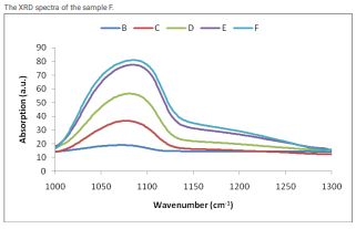
In our previous work (24), we got important results include the possibility of using the thermal oxidation ofsilicon in air to obtain Si/Si0, composites with controllable optical properties suitable for application inthe field of semiconductor device synthesis. On the other hand, we found that, the phenomena of splittingof transverse optical stretching and longitudinal optical vibrations effect on the optical absorptioncoefficient. In addition, we found that, the intensity of the XRD silicon peak is proportional to the relativeabsorption coefficient of amorphous SiO. Our present work is continuation of our previous work (24).Here. we attempt to probe the possible effects of the phenomenon of the splitting of londitudinal opticaand transverse optical stretching motions (observed in the infrared spectra of silicon oxide) on the opticaand structural properties of the Si/SiO, composites.

Fig1
We notice that, the plasma edge is proportional to the silicon peak position. The relationship betweenthem is linear except for the point corresponding to the sample F at which the regression of the splitincorocess happened. This result supports the relationship between the peak shift and the formation ofcrystal defects, which we deduced from Fig. 9. This is because the shift of the plasma edge towards shortwavelengths is associated with an increase in the concentration of conductive electrons (24,25). Theseelectrons belong to silicon nanoparticles resulting from breaking the long-range arrangement of thesilicon lattice as a result of the formation of crystal defects.