After many years as a hypothetical possibility, 3D IC stacking has emerged as a potential key enabler for maintaining semiconductor performance trends. Implementing 3D, however, will almost certainly require development of throughsilicon vias (TSVs), which in the past few years have been elevated by the semiconductor industry to the status of a crucial mainstream technology.
Producing these vertical connections can seem misleadingly straightforward: drill a blind hole through the silicon wafer, deposit a uniform liner layer of dielectric material to electrically isolate the via, deposit a barrier layer to prevent copper from diffusing into silicon, and then completely fill the via with electro-chemically deposited (ECD) copper. An additional copper-seed layer may be needed before via filling if the selected barrier material is too resistive to allow the inception of the ECD process; as we will see, this is the case for most dry-process barriers, but not for all barrier materials [1]. CMP and wafer-thinning steps conclude the sequence.
While the process flow is relatively simple, the industry's conventional approach to bringing it into volume production is, in essence, a patchwork attempt at implementing a revolutionary technology with an evolutionary attitude, using what's available today from other fields and pushing the envelope to make it work for TSVs. This strategy is encumbering the industry with unnecessary limitations in terms of technology performance, manufacturing infrastructure, and cost, as well as a longerterm issue that is potentially even more problematic: scalability.
But most importantly, designers want to make sure they don't have to completely redesign their ICs at every new node just because the TSV diameter cannot be scaled down accordingly. They need scalable TSVs, i.e., a technology allowing via size to shrink with each new generation without affecting the wafer thickness in the process − or paying a 40% premium every time the TSV shrinks [3].
With the dry-process approach, cost increases with aspect ratio (or, assuming the depth doesn't change, with decreasing via diameter): PVD is limited to AR <3:1; PEPVD can address AR<6:1, and iPVD can be used for AR<8:1. How do we tackle ARs at 20:1 and above? The only apparent alternative is expensive and low-throughput ALD.

Fig1
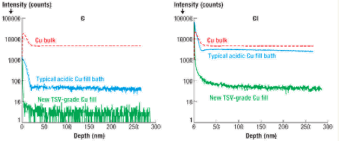
Contaminant levels have been measured by TOF-SIMS, focusing on C, S and Cl, and show much smaller values than typical acidic ECD chemistries, especially for chlorine (which is not part of the mildly basic chemistry formulation). Figure 3 shows an orderof-magnitude reduction in carbon contamination and a two orders-of-magnitude reduction in chlorine contamination for the new TSV-grade copper fill compared to conventional TSV chemistries.
Electrografting nanotechnology has been optimized for highly conformal growth of TSV films. The technology is fully compatible with standard semiconductor plating tools, enabling a large reduction in cost-of-ownership per wafer compared to the dry process approach [4], while also providing stable and well-monitored chemical baths. Film properties meet or exceed current TSV requirements, and chemical formulations are production-ready. TSVs manufactured using electrografting can be very narrow and have aspect ratios up to 20:1, thus broadening the 3D-IC design space and offering a process solution that can be extended for at least several generations into the future.