In this paper, a novel wet etched silicon interposer for optical interconnection applications has been proposed and fabricated. The interposer concept is conceived to include, via flip chip bonding, both CMOS ICs and optoelectronic dies to allow close proximity of electronics (drivers, TIAs) to photonics (VCSELs, PDs). The fabrication steps are developed to realize silicon recessed areas, to fit the semi-conductor circuitry, and openings to fit mechanical optical interface (MOI). Two steps of silicon anisotropic wet etch are performed to define these areas. The metal traces for electrical connection are designed to match the impedance for signal transmission and are lithographically defined. The obtained silicon interposer is shown and the process challenges discussed.
In the past few decades, the performance of data centres (DC) and High-performance computing (HPC) has been growing with an exponential rate [1]. To sustain this growth rate, it is projected that existing electrical interconnects in standard 19” width rack equipment connecting ASIC and pluggable transceivers on the front panel will be replaced by mid-board-optics (MBO) due to the front panel bandwidth density limits [2]. The footprint and the cost of the key modules (transmitter and receiver) are the main limitations, mostly due to the complex packaging. At present, the vertical-cavity surfaceemitting lasers (VCSELs) and surface normal photodetectors (PDs) arrays are the most promising photonic technology to realize transceivers. During the fabrication, the components are packaged on printed circuit boards (PCB), where dense integration is complicated and costly to assemble and fabricate. Besides, point-to-point wire bonding is employed to make the connections between the CMOS IC and optoelectronic dies, which increases the cost and suffers from limited RF performance [3].
Silicon is the preferred carrier to be used for packaging, because mature CMOS technology can be utilized. It provides a robust, reproducible and low-cost solution. In addition, silicon as interposer material has a coefficient of thermal expansion (CTE) similar to the dies used in the assembly, which prevents thermal related stress associated to the CTE mismatch [4]. Also, the way to fabricate the silicon interposer plays an important role in defining transceiver cost. Wet etching of silicon is preferred to dry etching since it is a standard low cost process, and double-side wet etching has been proposed to realize the electrical through silicon via (TSV) [5] which has played a key role in the progress towards 3D stacked ICs.
In this paper, we take advantages of silicon wafer scale process, and fabricate a novel silicon interposer by wet etching and double side-etching. The patterned silicon interposer is then gold plated to link the dense interconnections between the FR-4 PCB and the silicon ICs. Also, funnel-shaped TSV are realized to couple the laser light from a VCSEL to the mechanical optical interface (MOI) and Multiple-Fiber Push-On/Pull-off (MTP/MPO) connector.
The 2nd lithography is carried out on the already etched structure, after sputtering the seed layer for plating. The thick positive chemically amplified photoresist AZ® 40XT is employed for electro-plating. As shown in the Fig. 4(a), the photoresist is smoothly continuous after exposure and development of the photoresist: the light traces are the opening in the photoresist. A one micron thick layer of gold is then plated. Fig. 4b & c, shows the fan-out differential traces and short ground signal ground (GSG) traces between CMOS and VCSEL array after removing the seed layer.
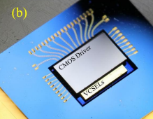
In order to make the funnel-shape TSV for light coupling, the last step of lithography is carried out on the backside using the same KOH wet etching process used on the front side. After 50 minutes, the remaining thin layer of silicon is etched through, and the optical windows are created (see Fig. 5a). The backside SEM photo (Fig.5c) shows the active region of VCSELs and the funnel-shaped optical windows, which will help to confine the light. The finished silicon interposer is shown in Fig.2e, and it is now ready to start the assembly of the optoelectronic and CMOS dies. A FINEPLACER® lambda die Bonder was employed to align the two chips. Firstly, we use gold-gold metal bonding between the pads on VCSEL and silicon interposer, with the thermal (300℃, 30s) compression (1N/pad) method. After that, the CMOS driver, with solder bumps on it, is placed and reflowed using the die bonder. The final assembled sample is shown in Fig.5b.

Fig1
In this paper, we demonstrated a new wafer level approach for optoelectronic packaging. We introduce the silicon interposer to connect the CMOS IC and optoelectronic dies, and make use of the both sides of the silicon interposer. One side is used for electrical connection, and the other side is used for optical connection, achieved by optical TSV.
In the future, the MOI will be mounted on the transmitter module, and the performances of the transmitter module can be tested. Further, the new processes for making the silicon interposer will be repeated on a thicker wafer, and deeper recessed area will be made to fully embed the CMOS chip. Thus, the optical engine will be more flexible and can be flipped on any carrier.
上一篇: III-V Si 光子通过芯片到晶圆键合
下一篇: 用于可扩展硅通孔的湿法工艺技术