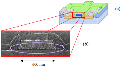
The overall quality of transistors is one of the leading issues in MOS (Metal Oxide Semiconductor) integrated circuits. This paper focuses on the gate-oxide layer of the MOS transistor and contains a comprehensive discussion of its quality using a 12.2 nm thick thermally grown gate-oxide. However to fully understand the impact of the gate-oxide layer it is important to review the transistors structure and operation to see just how much of its performance depends on the quality of its gateoxide.
The MOS transistor is a voltage controlled current source created through a semiconductor layering process. A simplified version of both NMOS and PMOS devices are shown in Figure 1 below along with a corresponding circuit representation. Structurally the transistor is composed of a bulk silicon substrate of type n or p (phosphorous or boron doped respectively) shown with connection B. An insulating layer of gate oxide is grown to isolate the polysilicon gate, with connection G, from the substrate material. Finally two implanted regions of n or p type silicon are added to created a source and drain area, connection S and D, respectively.
The fundamental principal of transistor operation is quite simple. For NMOS a positive voltage is applied to the gate, this begins to draw minority carriers, i.e. electrons, to the gate substrate interface, creating a conduction path between source and drain. A positive voltage applied to the drain (with source at ground) sweeps the electrons form source to drain creating ID, the fundamental current of interest in MOS operation. This is illustrated below in Figure 2.
At this point the importance of the gate-oxides insulating properties can be seen clearly. In theory the potential across the oxide draws carriers from the substrate to create a conduction path between source and drain with no current flowing into the gate. In reality however, some small amount of current does flow through the gate. If there are defects present in the oxide this current can begin to grow quickly as gate-voltage is applied. A set of criteria needs to be in place to identify the quality of a gate-oxide and its potential to be a perfect insulator.

Fig1
From above it can seen the great physical length current must flow in a transistor, in contrast to the extremely thin layer of oxide attempting to contain the current flow to the substrate alone, and not into the gate. Any small defect in such a thin layer of material could be catastrophic to the quality of the transistor. In order to project the quality of an oxide under normal operating conditions, full time dependent reliability of the SiO2 (gate-oxide) layer should be analyzed. This should include a complete charge-to-breakdown characterization of the oxide.
Oxide field strength as related to reliability is commonly plotted in a histogram, an example of which is shown Figure 4. With the independent variable the breakdown field strength, and the dependant variable breakdown frequency. Mode A failures are usually the result of gross processing mistakes (pin holes in the oxide, direct shorts, tester error) and are not solely considered a result of poor oxide; as such they will not be dealt with in this thesis. Mode C failures are called intrinsic failures and are inherent to every device. They are related to natural oxide deterioration. Oxide is gradually weakened by the passage of gate current. This weakening over time permits a continuous conductive path. At some point current will abruptly discharged through this path irreversibly breaking down the oxide. Mode B failures are considered defect driven, commonly referred to as extrinsic failure. Possible issues may be: contamination in the oxide film or substrate, surface roughness, thickness uniformity (localized thin oxide regions), crystalline defects in the substrate, or plasma-induced degradation.