Nano-porous silicon were simply prepared from p-type single crystalline silicon wafer by electrochemical etching technique via exerting constant current density in two different HF-Ethanol and HF-Ethanol-H2O solutions. The mesoporous silicon layers were characterized by field emission scanning electron microscopy and scanning electron microscopy. The results demonstrate that the width of nano-pores changes from 7 nm to 60 nm by varying current density from 10 mA/Cm 2 to 40 mA/Cm 2 , respectively and the depth of nano-pores also alters by applying different values of etching duration. It is concluded that varying current density leads to different width of pores while varying etching duration results in various depth of pores. Such etch tuning process is applicable for fabricating different nano-sized porous silicon for many modern electronic devices.
Silicon is a material with many particular molecular properties that can be a worthy candidate for many chemical devices such as sensing systems and anode materials for Li-ion battery [1-3]. Nevertheless, silicon is not considered a suitable material for many devices owning to its low surface area [4-5]. On the other hand, porous silicon (PSi) is currently a very applicable material due to its own unique surface, electrical and optical properties [6]. In general, porous materials are categorized into three classes according to pore sizes: macropore (above 50 nm in size), mesopore (50 – 2 nm) and micropore (below 2 nm) [7]. Recently, the synthesis of mesopore PSi has attracted increasing concerns because of its favorable characteristics for series of fabricating devices ranging from optoelectronics to electrochemical power sources.
Many fabrication techniques are specified to produce PSi [10]. In particular, electrochemical etch is the main method for fabricating PSi because electrochemical parameters of the process conditions obtaining better control of the physical features of the PSi. The method has benefits of being simple, repeatable and economic to produce PSi compared to vacuum-based thin film fabrication such as e-beam lithography.
Some researchers reported the diverse morphological structures of PSi electrochemically etched under varying the experimental parameters [11]. Kim and Cho reported the changes of the morphology of PSi are in relationship with the Si wafers and electrolyte resistance [12]. Depending on the electrical resistivity of Si wafers compared to that of the electrolyte, the fabrication of mesopores can be triggered at a critical current density [12]. The critical current density is changed when the composition of the electrolytes is varied.
In this study we investigated the change of morphological features of PSi samples under a range of electrochemical etching conditions, such as electrolyte composition and concentration, applied current density and etching duration. The morphological properties were scrutinized using field emission scanning electron microscopy (FESEM) and scanning electron microscopy (SEM) and were correlated to the etching parameters.

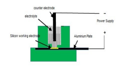
Fig1
To investigate the morphology of PSi, FESEM micrographs were obtained by a TSCAN MIRA3 microscope with high voltage ranging from 10 kV to 15 kV. The SEM images were also obtained by a Cambridge S360 microscope.
In electrochemical etching process, current density has an important effect on the width of pores for meso-porous Si samples. Figures 4-a to 4-d show FESEM micrographs of porous silicon samples with different current densities and with the same chemical ratio of 1:3 for HF/EtOH. Increasing the current density from 10 mA/Cm2 to 40 mA/Cm2 leads to increasing pore sizes from9 nm in Figure 4-a to 23 nm in Figure 4-c, respectively.
上一篇: 栅极氧化层完整性研究