A simple approach to wafer-scale self-cleaning antireflective hierarchical silicon structures is demonstrated. Byemploying the KOH etching and silver catalytic etching, pyramidal hierarchical structures were generated on thecrystalline silicon wafer, which exhibit strong antireflection and superhydrophobic properties after fluorination.Furthermore, a flexible superhydrophobic substrate was fabricated by transferring the hierarchical Si structure to theNOA 63 film with UV-assisted imprint lithography. This method is of potential application in optical, optoelectronic, and wettability control devices.
Nanostructured surfaces have attracted increasing attentiondue to their unique properties, such as superhydrophobicity andantireflection, which have promising applications in industry. Forexample, they can be applied for contamination prevention,biocompatibility, antioxidation,1 or improving the performanceof some optical and optoelectronic devices.2-4 Many efforts havebeen devoted to achieve the structured superhydrophobic orantireflective surfaces.4-16 From a practical standpoint, thecombination of superhydrophobicity and antireflection is moreattractive, especially on the silicon surface since they can beintegrated with other electronic components; for instance, themultifunctional silicon surfaces can increase the photovoltaicconversion efficiency of solar cells and prevent the device surfacesfrom being contaminated. So far, several methods have beenproposed to generate the multifunctional surfaces, including hierarchical etching,17 layer by layer,18,19 sol-gel process,20laser-induced damage of silica surface,21 fluorocarbon plasmananotexturing of polymer,22 and spin-coating technique.23 However, most of the methods are associated with problems, such asbeing time-consuming, complicated processes or expensive equipment, which will limit their applications. Therefore, a simple andcost-effective fabrication method for large area multifunctionalsurfaces is highly desired.
In this communication, we demonstrate a simple method forcreating hierarchical pyramidal structures on whole silicon waferusing chemical etching. The structured silicon wafer exhibitsstrong antireflective property in broadband wavelengths, whichalso shows superhydrophobic behavior after fluorination treatment. Furthermore, a flexible superhydrophobic surface can befabricated using imprint lithography with the hierarchicallystructured silicon as a stamp.

Fig1
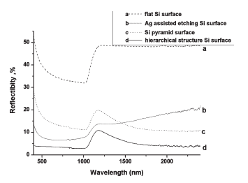
It is well-known that the high reflective index of silicon limitsthe performance of silicon-based optical and optoelectronicdevices, such as solar cells, displays, and light sensors. Herein,with the fabricated hierarchical structures, the reflectivity wasstrongly reduced. The antireflection comparison of the structuredand flat silicon wafers is shown in Figure 4. The diffuse reflectivitymeasurements indicate that up to 40% of the incident light isreflected on the flat silicon wafer (see line a in Figure 4). Bycreating the structured layers, a refractive index gradient isintroduced between air and the silicon wafer. The reflectancecan be reduced to 7% and 13% by the microscale pyramids andnanoholes on silicon surfaces, respectively, as shown in Figure 4(lines b and c), which can be further reduced to less than 4% byconstructing the hierarchical structures on the silicon surface (seeline d in Figure 4), and it can even be suppressed to 2.8% at the wavelength from 800 to 1100 nm. This method allows for a facilewafer-scale fabrication of a superhydrophobic and antireflectivesilicon surface, as shown in Figure 5. The different antireflectivebehaviors of the polished silicon wafer (left) and the hierarchicallystructured silicon wafer (right) can be easily observed from thephotographs. The polished silicon wafer is shinning, while thehierarchically structured one shows dark black.
上一篇: 硅纳米加工中KOH湿法蚀刻工艺的优化
下一篇: GaN晶体后处理及应用研究进展