The simple wet etching process for nanostructureformation seems straightforward. But, how far the wetetching process can be pushed so that it is applicable insilicon nanodevices and silicon nanostructureapplications. In terms of surface roughness andachievable feature size, the impact of aqueous KOH wetetching temperature was studied for nanostructureformation with (110) silicon wafer. The grid-linepatterns are generated by scanning probe lithography(SPL), which applied a bias between the tip and the(110)-oriented silicon wafer that results in an oxide hardmask for subsequent orientation-dependent etching(ODE) process. The etching rate is theoreticallyproportional to temperature the higher the temperaturethe higher the etching rate, whilst the surface roughnessand the nanostructures morphology deteriorated. Owingto the etching selectivity of (111)-plane/oxide decreasesas the etching temperature increases, it is found that theline-width of 20 nm nanostructure can be formed at 50℃ but with poor surface roughness morphology. For thesame etching depth, when the temperature changesfrom 50℃ to 30℃ the linewidth of nanostructureincreases from 29 nm up to 67 nm, but surfaceroughness decreases from 32 nm to 3.8 nm. It is alsofound that the additional agitation by ultrasonic cleanercan speed up mass transfer of chemical reactants onsurface of (110)-plane such that the surface roughnessand morphology are further improved. We havedemonstrated that: First, the optimization linewidth ofthe silicon nanofabrication can be reduced down to 20nm by using higher aqueous temperature than 30℃ andODE technique with ultrasonic agitation. Second, thesurface roughness of the wet etching with ultrasonicagitation is 3.282 nm which is comparable to that of dryetching (Rq = 2.101 nm) at the temperature 30℃.
Nanometer-scale structures and nano-fabricationtechnologies are investigated intensively recently. Themost widely used pattern-generation techniques areelectron-beam lithography (EBL) [1] and scanningprobe lithography (SPL) [2-5]. Electron beamlithography (EBL) is a well-established high resolutionpatterning technique in which high energy (10-100keV)electron are focused into a narrow beam and used toexpose electron-sensitive resists. Scanning probelithography (SPL) patterns on resist or conduct surfacewith high electric field forced the electrons or negativemobile ions from a sharp probe tip in close proximity toa the conduct sample. It is easily to print sub-50 nmfeatures using both systems, but SPL has widerexposure latitude at these small sizes. Also the SPL hasbeen proposed as a simpler and lower-cost alternative toEBL systems for the generation of nanometer-scalepatterns.
In this study, atomic force microscope (AFM) has beenemployed to generate nanometer-scale grid-lines andtransfer them into the material of interest. AFM inducedlocal oxidation of silicon is a process with a strongpotential for use in proximal probe nanofabrication.This system provides high resolution, which can beadjusted by tip/sample bias, set constant force (orconstant height), scanning speed, and ambient humidityof environment, without damage in the substrate [6-8].The patterns transferred into silicon employed theorientation-dependent etching (ODE) [9] method withthe potassium hydroxide solution (KOH). This processis chosen because of its excellent repeatability inmicro-fabrication and its low production cost, althoughthe surface roughness and morphology are detrimentalin nano-fabrication. In this study, we discussed therelationship between etching temperature, etching depthand linewidth. And we introduced the ultrasonicagitation to improve the surface roughness and thenano-structures morphology. Finally, the optimizationnano grid-line structures were demonstrated.
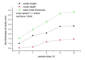
All experiments were performed with (110)-orientedsilicon wafer. The resistivity of the silicon substrate are around 1~10 ohm-cm. Samples were prepared by followprocess: standard RCA cleaning, native oxide removedand hydrogen passivated by dipping in 5% aqueoushydrofluoric (HF) solution before localized oxidationprocess by SPL. SPL was performed in air using thePark Scientific Instruments (PSI) Autoprobe M5 atomicforce microscope (AFM) operating with highly dopedsilicon cantilever tip (the tip radius is around 10~15 nm,the resistivity is around 0.01~0.025 ohm-cm). Thetip/sample force was held at 10nN (~0.01μm height). Avoltage bias between tip and sample generates theelectric field forced the electrons and negative mobileion (O-) penetrated into the sample.

Fig1
After the local oxidation, the orientation dependentetching process was introduced to obtain nanometerscale nanostructure. Because of the differentcrystalline-plane have the different quantity of chemicalbonds. So that the (111)-plane has the slowest etchingrate, that results in anisotropic etching with othercrystalline-plane. In this study, we also introduced theultrasonic agitation (43kHz), to improve the surfaceroughness and uniformity of the etching process. Finally,scanning electron microscope (SEM) was employed tocharacterize the surface morphology and measurementof nanometer-scale line-width.
Figure 5 demonstrates the etching rate of (110)-plane islogarithm proportional to the etching temperature inboth theoretical and experimental results. The (111)-plane etching rate dependent on temperature has beenalso demonstrated in this figure in the form of the linewidth shrinking when etching temperature increased. Asthe temperature rises from 30 ℃to 50 ℃ , for the sameetch depth the feature size of nano-structure shrinksfrom 70 nm to 30 nm. Temperature of aqueous KOHplays important role for both silicon etching and SiOxetching.
下一篇: 晶圆级自清洁抗反射硅表面的简单方法