Abstract—This work analyzes the influence of some chemical steps used in standard cleaning recipes on the surface micro-roughness of silicon wafers. The effect of varying the ammonium hydroxide concentration in the NH4OH: H2O2:H2O solution was studied and silicon wafer micro-roughness was characterized by atomic force microscopy technique at different scans of 1µmx1µm. Based on the results, it was possible to point the condition to obtain low surface micro-roughness for NH4OH-based solutions with the lowest NH4OH content before the growth of gate oxides. Following, it silicon-oxide thin films were grown onto periodic rectangular shapes, 100 nm in height, obtained by localized plasma etching on silicon wafer surfaces. Silicon oxides (SiO2), about 4.5 nm thick, were grown in ultrapure dry-O2 or pyrogenic (O2 + H2) environments in order to compare the planar uniformity and the grade of coverage at the step edges of rectangular shapes defined onto silicon surfaces. Pyrogenic and conventional oxidation at 850 oC allowed one to obtain gate oxides on 100 nm-stepped silicon surfaces with high dielectric breakdown field (>10 MV/cm), good planar uniformity and conformal coverage at the step edges. The impact of this result is now the feasibility of fabricating good-quality gate oxides for surrounding gate transistors (SGT’s) and texturized MOS solar cells.
I. INTRODUCTION
The search for the increase of the device integration in integrated circuits is characterized by a marked reduction in the vertical and horizontal dimensions. This reduction in the dimensions of the devices is accompanied by an improvement of their performance for surrounding gate transistors. Also, the reduction of the gate oxide thickness has become an important technological issue related to MOS solar cells.
Literature reports that less rough Si/SiO2 interfaces leads to lower leakage currents through the gate oxide layer, lower concentrations of traps at the Si-SiO2 interface and higher dielectric breakdown fields. Thus, in order to maintain or even increase the quality of the oxides, despite the reduction in thickness, greater care and greater control of the obtaining process is necessary. Parameters such as temperature, metallic contamination on the wafer surfaces or in the cleaning solutions, immersion speed of the wafers in the solutions and the hydrophilic or hydrophobic characteristic of the wafers, all affect the surface roughness before the gate oxidation. A parameter to be highlighted is the amount of NH4OH in the SC1 solution (Standard Cleaning 1). The smaller the amount of NH4OH, the longer the time required for the removal of particles. However, the NH4OH/H2O2/H2O solution in the proportion of 0.2/1/5, after 10 minutes, shows the same efficiency in the removal of particles as in the proportion of 1/1/5, while the reduction in the concentration of NH4OH is followed by a reduction in the surface roughness of silicon wafers.
II. EXPERIMENTAL PROCEDURES
First, it was analyzed the solution that constitutes the first part of the known RCA cleaning which in turn is known as standard cleaning number 1 (SC1 - Standard Cleaning 1). Below, the description of four variations of the SC1 with four concentrations of NH4OH and two temperatures (71oC and 84oC) are presented.
For all tests, 3-inch p-type wafers were used, doped with boron, orientation <100>, resistivity in the range of 1 to 10Ωcm and thickness of 381±5µm. These wafers were cleaved into four equal parts and each of these parts was assigned to each of the solutions described. The different solutions were heated to reach different temperatures (71o and 84oC) and the pieces of wafers were individually immersed for 15 min. in these solutions. To obtain better temperature control and minimize a possible imbalance caused by preferential evaporation of a certain component (H2O2 or NH4OH), a glass lid was used over the beaker with a hole through which a thermometer was placed to control the temperature. After immersion in the different solutions, the samples were rinsed in DI water for 5 min., followed by drying in a ultrapure nitrogen jet. The time interval between the end of the sample preparation and the atomic force microscope (AFM) analysis was approximately 12 hours. During this time interval, the samples were placed in a properly cleaned glass sample box, which in turn were kept in a clean room environment until the AFM analysis. Then, using AFM, the surface roughness values were obtained. For the atomic force microscopy analysis, the equipment “Atomic Force Microscopy – Nanoscope E Digital, Inc.” was used.
In the moment that preceded the AFM measurement, the samples were then cleaved into pieces of approximately 1 cm x 1cm to be positioned on the sample holder of the Nanoscope. Then 1 µm x 1µm scans were measured using a standard silicon nitride tip, also from Digital. The interaction force observed between the sample and the surface was approximately 50nN. The 4 samples that underwent to the different cleaning solutions based on NH4OH were dipped in 40H2O : 1HF for 30 s, followed by a rinse in DI water for 60 seconds to remove the native oxide. Then, these samples were analyzed by atomic force microscopy in the same way already described.
Following, gate oxides were grown on flat and with vertical steps (trenches). The depth of the steps was set at 100 nm, which is about an order of magnitude greater than the thickness of the oxide to be grown. Figure 1 schematically illustrates the MOS capacitor on an irregular surface formed by trenches with height h = 100 nm on which gate silicon oxide was grown. The fabrication process of MOS capacitors was based on the previous analysis of the cleaning procedures using the baths 1, 2, 3 and 4 and a complete recipe for chemical cleaning will be proposed as a modification of a standard RCA cleaning for the gate pre-oxidation process, which will be presented in the Results and Discussion.
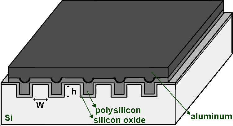
Fig. 1 - Schematic representation of the MOS capacitor with an area of 300 μm x 300 μm manufactured on an irregular surface composed of trenches with height h = 100 nm and width W = 30 μm.
III. RESULTS AND DISCUSSION
Tables II and III show the surface roughness results RMS (RRMS), mean (Ra) and valley-peak (Rv-p max), obtained for the samples that were underwent to the different solutions SC1 at different temperatures for scanning 1µm x 1µm.

TABLE II
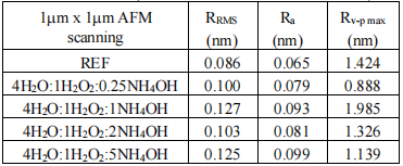
TABLE III
Figure 2 shows 3D images of the reference sample (asreceived wafers without any treatment (REF+) and of the sample processed in 4H2O:1H2O2:0.25NH4OH at 71oC during 15 min followed by dip in 1HF:40H2O during 30s for a scan area of 1 μmx 1μm. It is important to point out that the removal of the native oxide after immersion in 4H2O:1H2O2:0.25NH4OH at 71oC for 15 min means low roughness parameters (RRMS, Ra and Rv-p max) in the Table IV with the lowest content of NH4OH.
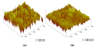
Fig. 2 - 3D images obtained by AFM in 1 μm x 1 μm areas for : (a) asreceived wafer (no treatment), (b) sample processed in 4H2O:1H2O2:0.25NH4OH at 71oC for 15 min followed by dip in 1HF:40H2O during 30s.
Figure 3 shows the RMS roughness for the different samples (as-received, and the samples that underwent to the baths 1, 2, 3 and 4 indicated in Tables II, III, IV and V) and the two bath temperatures used. Figure 4 corresponds to the same samples processed after immersion in dilute HF solution. In addition to the substantial reduction in surface micro-roughness after the native oxide removal, lower micro-roughness is observed at 71oC for samples that did not undergo the dip in HF diluted solution, possibly due to surface oxidation with a greater degree of unevenness promoted by the OH species at lower temperatures.
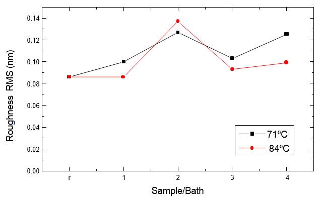
Fig. 3 - RMS roughness obtained by AFM for samples 1, 2, 3 and 4 and reference as indicated in Tables II and III.
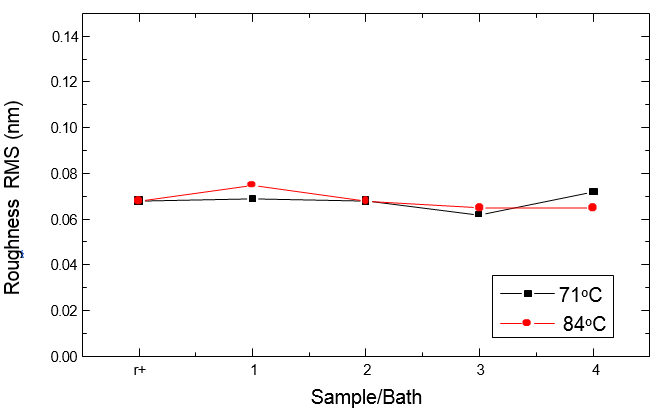
Fig. 4 - RMS roughness obtained by AFM for samples 1, 2, 3 and 4 and reference as indicated in Tables II and III.
IV. CONCLUSION
Thin films of silicon oxide were grown on surfaces of silicon wafers containing periodic rectangular shapes with 100 nm in height. Silicon oxides (SiO2) about 4.5 nm thick were grown in ultrapure oxygen (O2) or pyrogenic (O2 + H2) environments. It was shown that pyrogenic or conventional oxidation at a temperature of 850oC allows obtaining gate oxides on steps with a high breakdown field (>10 MV/cm), good planar uniformity and good coverage at the edges of the steps.