通过化学镀镍沉积增强纳米多孔硅光电阴极的光电化学性能
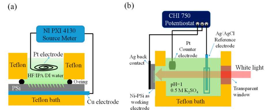
Renewable energy sources, particularly solar energy, are key to our efforts to decarbonize.This study investigates the photoelectrochemical (PEC) behavior of nanoporous silicon (NPSi) and its Ni-coated hybrid system. The methods involve the application of a Ni coating to NPSi, a process aimed at augmenting catalytic activity, light absorption, and carrier transport. Scanning electron microscopy was used to analyze the morphological changes on NPSi surfaces due to the Ni coating. Results demonstrate that the Ni coating creates unique structures on NPSi surfaces, with peak PEC performance observed at 15 min of coating time and 60 ◦C. These conditions were found to promote electron-hole pair separation and uniform Ni coverage. A continuous 50-min white light illumination experiment confirmed stable PEC fluctuations, showing the interplay of NPSi’s characteristics and Ni’s catalytic effect. This study provides practical guidance for the design of efficient water-splitting catalysts, contributing to the broader field of renewable energy conversion.

钙钛矿薄膜和单晶的合成方法
Halide perovskites are compelling candidates for the next generation of clean-energy-harvesting
photovoltaic technologies owing to an unprecedented increase in power conversion efficiency and their low cost, facile fabrication and outstanding semiconductor properties. The potential of perovskite materials has been identified by understanding the fundamental science of perovskites such as crystallisation dynamics and charge carrier dynamics and finding various novel perovskite combinations from the periodic table. Current evidence suggests that the synthetic approach applied for the deposition of halide perovskite layers is a key factor dictating device efficiency and stability. In this review, we aim to investigate the large variety of synthetic procedures followed for the deposition of perovskite polycrystalline films and single crystal layers. We will summarize the current understanding and ability to influence material properties by using these synthetic methods and explore the link between synthetic approaches and material properties relevant to photovoltaic and other applications.

金属有机化学气相沉积 III 族氮化物半导体同质外延及其对垂直器件影响的综述
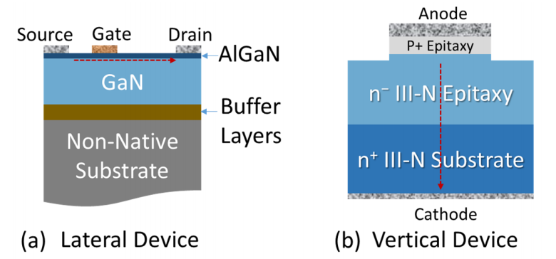
This paper reviews some of the basic issues in homoepitaxial growth of III-nitrides to enable a vertical device technology. It focuses on the use of metal organic chemical vapor deposition (MOCVD) to grow GaN and explores the effects of the native substrate characteristics on material quality, interface composition, and device performance. A review of theoretical work understanding dopants in the ultra-wide III-nitride semiconductors, AlN and BN, is also included for future efforts expanding the technology into those materials.

关键词:光电化学,纳米多孔,化学镀镍沉积,钙钛矿薄膜,钙钛矿单晶合成方法,氮化镓,AlN,同质外延,MOCVD,二极管,金属有机化学气相沉积,垂直器件