Abstract
Silicon photonics has emerged as a mature technology that is expected to play a key role in critical emerging applications, including very high data rate optical communications, distance sensing for autonomous vehicles, photonic-accelerated computing, and quantum information processing. The success of silicon photonics has been enabled by the unique combination of performance, high yield, and high-volume capacity that can only be achieved by standardizing manufacturing technology. Today, standardized silicon photonics technology platforms implemented by foundries provide access to optimized library components, including low-loss optical routing, fast modulation, continuous tuning, high-speed germanium photodiodes, and high-efficiency optical and electrical interfaces. However, silicon’s relatively weak electro-optic effects result in modulators with a significant footprint and thermo-optic tuning devices that require high power consumption, which are substantial impediments for very largescale integration in silicon photonics. Microelectromechanical systems (MEMS) technology can enhance silicon photonics with building blocks that are compact, low-loss, broadband, fast and require very low power consumption. Here, we introduce a silicon photonic MEMS platform consisting of high-performance nano-opto-electromechanical devices fully integrated alongside standard silicon photonics foundry components, with wafer-level sealing for longterm reliability, flip-chip bonding to redistribution interposers, and fibre-array attachment for high port count optical and electrical interfacing. Our experimental demonstration of fundamental silicon photonic MEMS circuit elements, including power couplers, phase shifters and wavelength-division multiplexing devices using standardized technology lifts previous impediments to enable scaling to very large photonic integrated circuits for applications in telecommunications, neuromorphic computing, sensing, programmable photonics, and quantum computing.
Introduction Photonic integration holds promise for combining complex optical systems onto a single chip, and over the past decades, significant progress towards this goal has been achieved. Several material and technology platforms have reached industrial maturity. Among the most widely adopted technology platforms are planar lightwave circuits (PLCs) , indium phosphide (InP), silicon nitride (SiN), and silicon photonics. Research further explores additional material platforms, such as lithium niobate, aluminium nitride and single crystal diamond, by virtue of the material’s high electro-optic coefficient, strong piezo-electric effect, or potential to host colour centres as single photon sources, respectively. Although these efforts are of high potential and interest, particularly for quantum photonics, significant progress is still required to achieve industrial maturity.
The choice of a material and technology platform is driven by specific application requirements. For example, fibre-optical telecommunications has been a driver of near-infrared photonic integrated circuits, such as integrated arrayed waveguide gratings that are primarily built in planar lightwave circuits. These low absorption and high-quality waveguides enable very low loss, yet the low-index difference of the silica waveguides leads to relatively large bend radii and thus limits further miniaturization. In addition, PLC technology provides only passive photonic components. Silicon nitride waveguides have recently gained interest due to their significant advancement in reducing on-chip propagation losses and ability to support wavelengths in the visible and nearinfrared range for imaging applications; however, current silicon nitride technology platforms only support passive elements. Conversely, indium phosphide-based integrated photonics allow for the integration of active components, including laser sources and photodetectors alongside waveguides and passive components. However, III–V semiconductor wafers remain expensive and limited in size, hitherto prohibiting cost-efficient very large-scale integration.
Silicon photonic microelectromechanical systems (MEMS) technology can simultaneously overcome all these limitations. For example, one of the largest-scale PICs today, a 240 × 240 silicon photonic switch matrix with 57,600 individual switching elements, has been demonstrated experimentally by combining MEMS with silicon photonic waveguides. MEMS itself is a mature technology, and billions of MEMS micromirrors, microphones, accelerometers, gyroscopes, etc., reliably power countless consumer electronic devices. The combination of MEMS with integrated photonics, however, requires specific engineering and process integration. The recently demonstrated large-scale silicon photonic MEMS switch matrix and large-scale silicon photonic MEMS LiDAR clearly show the potential of the combination of silicon photonics and MEMS. Yet this specific technology requires multilayer stacking of waveguides, and the involved high-temperature deposition processes make it challenging to be compatible with standard silicon photonic components such as high-speed modulators and photodiodes. The potential of silicon photonic MEMS has also been recognized in early work that focuses on demonstrations of individual devices. For example, phase shifters, switches, tunable ring resonators, optomechanical photonic crystal cavities and compact optomechanical ultrasound sensors have been demonstrated as individual devices or small-scale circuits in single-layer silicon photonics. Figure 1 summarizes a selection of hitherto experimentally demonstrated individual silicon photonic MEMS devices (Fig. 1a–c) and a selection of recently demonstrated scaled silicon photonic MEMS for beam steering (Fig. 1d) and switching in datacentres (Fig. 1e, f). A more complete account of previously demonstrated silicon photonic MEMS can be found in a recent review.
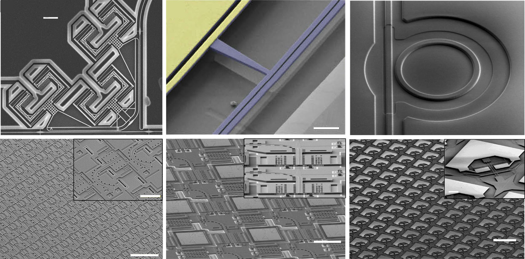
Fig. 1 Representative examples of recently demonstrated silicon photonic MEMS. Individual components based on dedicated processes on silicon-on-insulator wafers include a tunable couplers, b phase shifters, and c ultrasound sensors, and silicon photonic MEMS based on specifically developed microfabrication processes using multiple layers have shown d beam steering for 3D imaging and e, f large-scale photonic switch matrices for optical circuit switching in datacentres. (Permissions: a Adapted with permission from ref. © The Optical Society. b Adapted with permission from ref. © The Optical Society. c Adapted with permission from ref. © Springer Nature. d Adapted from ref. under creative commons license CC BY 4.0. e Adapted with permission from ref. © The Optical Society. f Adapted from ref. under creative commons license CC BY 4.0)
To introduce MEMS into standardized silicon photonics, the waveguides must first be made movable, and the MEMS actuators must second be implemented. Finally, to protect MEMS structures from environmental influences and for handling without the risk of damage, we have developed a wafer-level sealing process that allows placement of thin caps above the MEMS cavities. A simpli- fied schematic cross-section of our silicon photonic MEMS technology platform is shown in Fig. 2a.
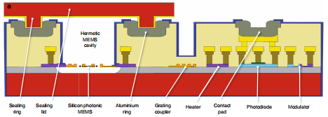
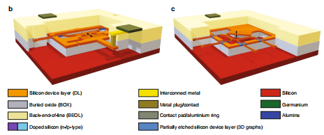
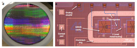
Fig. 2 Integrated silicon photonic MEMS technology platform. The platform is based on IMEC’s iSiPP50G platform, enhanced with custom postprocessing to produce suspended and movable MEMS structures alongside the platform’s standard components and with sealing caps above the MEMS structures to provide protection of the movable MEMS devices. a Schematic cross section of the technology platform and 3D perspective views of b in-plane and c out-of-plane movable devices to visualize conceptually the electrostatic actuators, the optical and electrical routing, as well as grating coupler and metal contact pads, serving as interfaces. d Photograph of a 200 mm silicon photonics wafer before MEMS release postprocessing and e microscope recording of a representative MEMS device integrated alongside high-performance grating couplers, low-loss waveguides for optical routing, and two metal levels for electrical routing. The final metallization layer serves as a bond pad for wirebonding, as well as an aluminium ring for the wafer-level hermetic sealing process.
In principle, a variety of MEMS actuation methods, such as electrothermal, electromagnetic, or piezoelectric actuation, can be implemented in photonics. Here, we choose electrostatic actuation due to the relative ease of process integration and lower power consumption compared to electrothermo-mechanical actuators. In particular, electrostatic actuators can be readily implemented using doped silicon as actuator electrodes, while electromagnetic or piezoelectric actuators require the integration of additional magnetic or piezoelectric materials, which are currently not available in standardized integrated photonics. Accordingly, we have developed a dedicated postprocessing procedure applied to the foundry processed silicon photonic integrated circuits that removes the sacrificial buried oxide selectively in the MEMS areas, as detailed in the methods section. We have implemented electrostatic actuators leveraging silicon device layer doping and electrical interconnects by metal routing layers to bond pads. Using a bias voltage between the handle layer and the device layer, an out-of-plane movement is achieved, while applying a voltage between two electrodes in the device layer induces in-plane displacement. The concepts for both in-plane and out-of-plane MEMS actuation in silicon photonics are shown schematically in Fig. 2b, c, respectively.
We fabricated our photonic MEMS design using the standard iSiPP50G platform that is processed on full 200 mm wafers, as shown in Fig. 2d. Our MEMS components are integrated alongside any of the highperformance library components available in the process design kit (PDK). A representative photonic MEMS device is shown in the microscope image of Fig. 2e, alongside several platform components, such as highperformance grating couplers, waveguide routing, twolevel metal routing for electrical interconnects, and final metallization that is used for both the external electrical interfaces (bondpads) and for the wafer-level hermetic sealing process. To demonstrate the capabilities of our silicon photonic MEMS platform, we present a selected set of representative, experimentally demonstrated key functionalities exploring physical displacements at the microscale and nanoscale: optical power distribution and switching, phase shifting, and wavelength selective operations.
MEMS actuation increases the vertical gap separation between the movable and fixed arms of the coupler, thereby effectively decreasing the optical power coupling. Based on this operating principle, in the unactuated state, light injected at the input port shown in Fig. 3a couples completely over the first directional coupler and then again in the second coupler, exiting at the drop port. When the actuator is engaged such that it has been displaced approximately 300 nm down towards the substrate, there is no coupling in the first directional coupler, and all the optical power exits the device at the through port.
Figure 3b shows a fabricated tunable coupler after the MEMS release postprocessing step. The footprint of the device is 78 µm × 78 µm. The release process results in a well-released device without visible residues and with both directional coupler pairs well aligned, which indicates low residual stress in the suspended waveguides. Optical characterization results are shown in Fig. 3c. In the idle, nonactuated state (0 V actuation voltage), the optical power is sequentially coupled from the input port through the two directional couplers to the drop port. At the operation wavelength, an extinction ratio of 25 dB is achieved between the drop and the through port. In the actuated state (27 V), optical power is concentrated in the drop port, with an extinction ratio of 30 dB with respect to the drop port. The 3 dB spectral bandwidth of the device is >30 nm. The actuation voltage for vertical actuators can be reduced by using a softer suspension design, with the trade-off of increased footprint and increased response time, and we have previously demonstrated vertically actuated silicon photonic MEMS switching with an actuation voltage as low as 3.75 V.
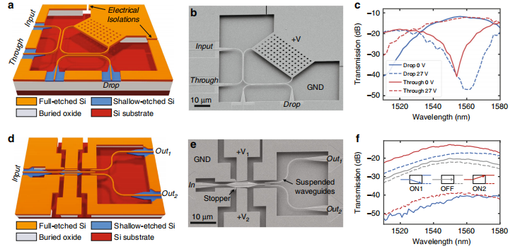
Fig. 3 Tunable power couplers and switches. a 3-D schematic view of an out-of-plane actuated tunable power coupler indicating the input, through, and drop ports and the actuator. b SEM recording of the released device showing a cleanly suspended and initially well-aligned configuration of the couplers in the unactuated state. c Measurement results for the spectral characteristics of the tunable power coupler under DC actuation showing a maximum extinction ratio of 25 dB between the drop and through ports in the unactuated (0 V) state and a maximum extinction ratio of 30 dB in the actuated (27 V) state. The associated 3-dB bandwidth of this device is >30 nm. d 3-D schematic view of an in-plane actuated photonic 1 × 2 switch with the movable input and two fixed outputs. e SEM recording of the released device showing the curved electrodes, stoppers, and suspended waveguides. f Measurement results for the spectral characteristics of the device in all three functional states: ON1, OFF, and ON2, wherein the extinction ratio is >23 dB for both ON states and the bandwidth is >70 nm.
Wafer-level hermetic sealing of the silicon photonic MEMS
Nearly all silicon photonic MEMS devices feature suspended and movable parts, including the devices presented above. To ensure reliable operation and protect suspended silicon photonic MEMS devices from environmental influences, such as dust and varying humidity levels, the devices must be placed inside hermetically sealed cavities. Therefore, we have developed a platform for wafer-level hermetic sealing of silicon photonic MEMS by wafer bonding. This approach is a wafer-scale process utilizing commercial semiconductor wafer bonding equipment. It is fully compatible with the PIC silicon photonic foundry platform (iSiPP50G, IMEC) and features optical and electrical feedthroughs from the inside to the outside of the hermetically sealed cavities containing the silicon photonic MEMS.
上一篇: 晶硅片各向异性表面制绒工艺实验分析
下一篇: 基于氢氧化钾各向异性刻蚀的高固硅微针制备