ABSTRACT
The development of silicon devices, circuits, and systems in most cases relies on the wet-chemical etching of silicon wafers (SWs). To achieve deep etching and micromachining, shaping, as well as cleaning, the dissolution of silicon using liquid chemical solutions is imperative. This study reports an experimental investigation of surface texturing of silicon wafers using a mixture of aqueous potassium hydroxide (KOH) solution and isopropyl alcohol (IPA) as a complexing agent to enhance light absorption and reduce the optical reflectance in the visible spectrum. Crochralski (CZ) silicon wafers of 100 mm diameter, 2” <100>-oriented, n-type, resistivity (Ωcm) of 7-21, with polished and lapped surfaces were utilized in the experiment. The process variables investigated included temperature (60 – 90) °C, duration of etching time (30 – 60) mins and concentration of KOH and IPA of (1 - 4) mg/l for KOH and (2 – 8) mg/l for IPA. The properties of the etched and unetched silicon wafers in terms of morphology, structure, photoluminescence, and electroluminescence were investigated to determine the effects of the process parameters on the efficiency and structural properties of the textured wafers. The SEM measurements revealed the presence of localized roughening pyramidal images. This showed that the use of KOH and IPA solutions on the silicon wafers revealed pyramidal structures that can be used to control the optical reflectance of the silicon wafers due to light scattering by the localized roughening. The applied etching procedure also produced low-reflecting materials whose reflectivity increases with wavelength. This study shows that textured material has great potential in optoelectronic device manufacturing processes.
1. Introduction
The study of crystalline silicon has a very important role in modern science and technology due to its excellent properties. It is generally known that about 90% of the solar panels used worldwide are comprised of silicon-based cells. The high refractive index exhibited by silicon usually leads to optical losses in solar panel manufacturing. Mostly, the rays absorbed from the sun are moderately weak. Due to these optical losses, the efficiency of crystalline silicon solar cells reduces to a level which is usually between 12 and 20 % . There have been concerted efforts geared towards improving the efficiency of solar cells based on silicon materials by exploring greater opportunities in developing reflection-reduction technologies to enhance better absorption of incident sun rays and invariably, improve crystalline solar cell. Though the thermodynamics of these solar cells are not easy to figure out, they have been extensively utilized in the production of optoelectronic devices . There are also frequent and increasing applications in nano-electronics, communications, solar cells, etc . However, of all the anticipated applications of crystalline silicon, solar cells (photovoltaic) are the most attractive form owing to their advantages over conventional sources of energy (fossil fuels). As an eco-friendly and clean supply of energy, the effects of pollution resulting from the incomplete combustion of fossil fuels are eliminated. Unfortunately, the high optical losses and low efficiencies of silicon solar cells make them less competitive. In achieving efficiency in silicon solar cell manufacturing, the requirement for the uniformity of textured surfaces is imperative. This can be undertaken through texturing the surface of the crystalline wafer using anisotropic etching to transform or alter the silicon’s surface parameters into different structures. In so doing, there is a reduction in reflection and enhancement in the absorbed incident light onto the silicon wafer.
2. Methodology
The procedures adopted for the texturing of the silicon wafers were those reported by Fashina et al and King and Buck The texturing experiment was conducted using aqueous solutions of KOH and IPA as the complexing agents. The IPA facilitates the texturing process by dissolving hydrous silica formed at the reaction interface. Czochralski (CZ) silicon wafers of 1 μcm resistivity, polished and lapped surface were used for the investigation. The CZ silicon wafers used for the experiment were 100 mm in diameter, <100>-oriented, n-type doped, thickness of 250μm, resistivity (Ωcm) of 7-21, with the polished and lapped surface. The process variables investigated were temperature, time and IPA and KOH concentrations. The ranges considered were: time (30 – 60) mins; temperature (60 – 90C and etchant concentration (KOH – IPA): (1-4) mg/l – (2 – 8) mg/l. The study was conducted using a 250 ml flat-bottom flask containing the KOH solution. The etching process was performed at different etchant concentrations, times and temperatures in an electrical thermostatic water bath boiler with reciprocating motion.
3. Results and Discussion
3.1 Surface Profilometry
Stylus surface profiler is a useful characterization technique for the determination of the size and surface roughness of Nano-materials. The technique aids in determining the presence of aggregates, voids, and homogeneity orientation with respect to the surface. On the other hand, the roughness (surface) of any silicon wafer is an important parameter in semiconductor characterization. It influences the mobility as well as the optical and electrical properties of the wafer for device applications. The average roughness of the etched wafers is given in Tables 1, 2 and 3 for the various properties investigated on the textured SWs. The values obtained at the various process parameters are in agreement with other studies conducted on the dependence of wafer reflectance and etching time. Table 1 indicates that the average roughness of the etched-SWs increased with the etching time. The gradual increase in surface roughness with etching times corresponds with the reflectance result of less than 10% achieved in literature for silicon materials. Table 2 shows that there was a corresponding increase in the roughness of the etched-SWs as the etching temperature was increased. The magnitudes of the values are similar to those reported in the literature for etched silicon wafers.


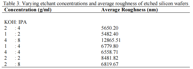
Table 3 shows the effects of varying the etchant concentrations in the etched silicon wafers. From table 3, it was observed that the average roughness of the wafers was significantly influenced as the etchant concentration varied around the optimum values of 2:4. The average roughness was affected by both the amount of KOH and IPA present in the reacting mixture as well as on the textured wafers.
From Tables 1 and 2, it was observed that the average roughness of the etched wafers was increasing correspondingly with time and temperature. The main effect of these parameters (time and temperature) on the surface roughness is significant, as higher time and temperature produced rougher surfaces. Similar observations have been reported in the literature and were due to the presence of defects within the wafers system.
3.2 SEM Analysis
Surface topology is used to understand the morphological characteristics or behaviour of etched silicon wafers and its role cannot be overemphasized. Scanning electron microscopy (SEM) morphology studies provide an understanding of the nature of the textured surface and are an important qualitative parameter in any study. Figure 1 shows the surface morphological patterns of the textured material at various etching times. Generally, it was observed that the materials were well-covered with different morphological structures. From the figure, the SEM textured images show an increased pyramid of grains that are randomly distributed. However, a further increase in textured time leads to the formation of various pyramidal grains with different morphological structures. Partially dense and compact nano-grains covering parts of the substrates are formed for A (Figure 1(a)). As the deposition time increases, the pyramidal grains increase in size with an agglomeration of clusters, as indicated in Figure 1(B) for B. After 50 minutes (Figures 1(C and D)), the clusters of larger grains metamorphose into smaller numbers of particle-like, rough, and irregular pyramidal grains. The development of various morphological features was due to the variation in nucleation rate as the texturing time increased. This enhancement shows that varying the textured duration results in several pyramidal grains coalescing and diffusing simultaneously to form the variously defined morphologies.
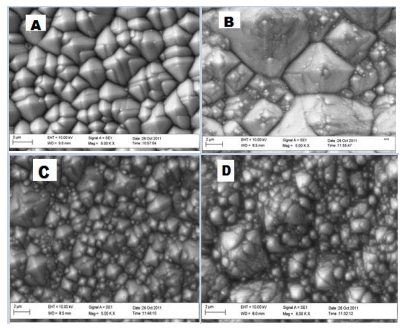
Figure 1. SEM textured image of silicon wafers at optimum etching time (A) 30 Mins (B) 40 Mins (C) 50 Mins (D) 60 Mins
The SEM images of the temperature-dependence nature of the etched silicon wafers are shown in Figure 2 for the various temperatures. It can be observed that the substrates were well-covered with films of different morphological structures. For 60 ᴼC, the SEM micrograph shows rough and wellcovered pyramidal images, which indicates the formation of a complete grain within the films. Increasing the deposition temperature to 70 ᴼC, it was observed that the films were rougher with the formation of some compact grain-like features. The gradual formation of smaller grain-like features was due to the increased nucleation rate as the deposition temperature increased. Further increase in deposition temperature from 70 ᴼC to 80 ᴼC, increased the formation of the pyramidal grain sizes. The SEM images corroborate the results obtained by the surface profile studies. However, at 90 °C, the SEM image indicated surface damage showing that beyond 80 °C etching temperature, the etching process was destructive on the silicon wafers.
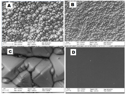
Figure 2. SEM textured images of silicon wafers at optimum temperature (A) 𝟔𝟎𝟎 𝐂 (B) 𝟕𝟎𝟎𝐂 (𝐂) 𝟖𝟎𝟎 𝐂 (𝐃) 𝟗𝟎𝟎 𝐂
Figure 3 shows the SEM textured images of the surface morphologies at different concentrations for the silicon wafers. The pyramids produced were of different sizes when compared to that in Figure 1. Correspondingly, Park et al have reported similar observations for crystalline silicon due to concentration modulations. Furthermore, the different morphological structures exhibited by the material may be the direct consequence of the variation in concentration and surface roughness exhibited by the material.
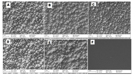
Figure 3. SEM textured images of silicon wafers at mixture concentrations (A) 1:2:46 (KOH:IPA:DI) (B) 1:2:46 (KOH:IPA:DI) (C) 2:4:46 (KOH:IPA:DI) (D) 2:4:46 (KOH:IPA:DI) (E) 4:4:46 (KOH:IPA:DI) (F) 4:4:46 (KOH:IPA:DI)
3.3 Effect of process parameters on the textured silicon wafers
Figure 4 shows the dependence of the reflectance of the textured wafers on the etching time. It was observed that the reflectance decreased as the etching time increases reaching an optimum value at 40 min etching time. Further increase in time beyond this optimum time has no significant effect on the reflectance as shown in Figure 4.
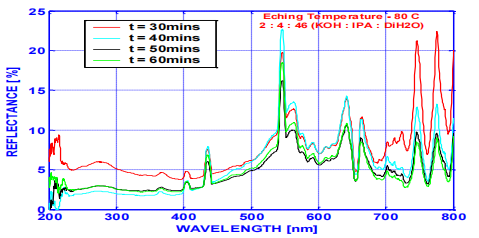
𝐅𝐢𝐠𝐮𝐫𝐞 𝟒 𝐑𝐞𝐟𝐥𝐞𝐜𝐭𝐚𝐧𝐜𝐞 𝐬𝐩𝐞𝐜𝐭𝐫𝐚𝐥 𝐨𝐟 𝐭𝐞𝐱𝐭𝐮𝐫𝐞𝐝 𝐬𝐢𝐥𝐢𝐜𝐨𝐧 𝐰𝐚𝐟𝐞𝐫𝐬 𝐰𝐢𝐭𝐡 𝐞𝐭𝐜𝐡𝐢𝐧𝐠 𝐭𝐢𝐦
4. Conclusion
In this study, process variables have been identified such that the results show low-reflectance properties and surface textures which are compatible with optoelectronic devices as well as other solar cell fabrication processes. Minimizing the reflection loss from the front surface of a solar cell is the most important reason for surface texturing activities. Notwithstanding this salient reason, several other factors must be placed into consideration in ensuring that the texturing system is compatible with other solar cell production procedures and processes to achieve minimal cost implications. Furthermore, an operational surface texturing process at 80 °C and low concentrations of KOH and IPA was established. The etching process, using the solution of KOH: IPA produced pyramidal shapes of different dimensions. The average roughness of the etched silicon wafers was within a broad range of values of less than 10 % in all etched samples. The SEM analysis confirmed the pyramidal nature of the grains that are influenced by the surface roughness. The reflectance increased with wavelength as well as etching time and temperature indicating that the texturing technique has the potential to be adapted to solar cell fabrication. Thus, the texturing process applied to silicon wafers provided an enhanced surface structure in terms of morphology and reflectance which can be used in solar cell applications.
上一篇: 流速对微流控芯片中层流的影响
下一篇: 集成硅光子 MEMS