Abstract.
The quality of the silicon carbide (SiC) epitaxial layer, i.e., layer homogeneities and extended defect densities, is of highest importance for high power 4H-SiC trench metal-oxidesemiconductor field effect transistors (Trench-MOSFET) devices. Especially, yield for devices with a large chip area is severely impacted by extended defects. Previously, devices had to be fully manufactured to effectively gauge the impact of a reduction in extended defect densities in the epitaxial layers on device yield. The production of devices such as Trench-MOSFETs is an extensive procedure. Therefore, a correlation between extended defects in the epitaxial layer and electrical device failure would allow to reliably estimate the impact of process changes during epitaxial layer deposition on electrical device yield.
For this reason, n-type epitaxial layers were grown on around 1,000 commercially available 150 mm 4H-SiC Si-face substrates, which received a chemical wet cleaning prior to the epitaxy deposition. Substrates with lowest micro-pipe density from two different suppliers were used. The wafers were characterized with the corresponding device layout for defects utilizing surface microscopy as well as ultraviolet photoluminescence techniques. Subsequently, these wafers were used to produce more than 500,000 Trench-MOSFET devices. All devices have been tested on wafer level for their initial electrical integrity.
Introduction
Silicon carbide (SiC), especially the 4H poly-type, possesses superior physical, electrical and thermal properties compared to silicon. These properties result in an increasing commercial interest of SiC as a material for high-power and high-voltage semiconductor devices. Thus, small and efficient SiC devices, e.g., trench metal-oxide-semiconductor field effect transistors (Trench-MOSFETs) in high-power inverter modules, are steadily replacing established silicon technologies.
Experimental Procedure
Commercially available 150 mm 4H-SiC substrates with off-cut angle of 4° towards the direction were used for this investigation. Homo-epitaxial layers were grown using a multi-wafer warm-wall chemical vapor deposition epitaxy reactor. All n-type layers were grown on “epitaxy-ready” polished and wet chemical cleaned Si-face substrates with low micro-pipe density.
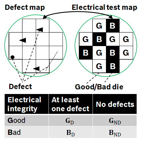
In Fig. 1 the four possible categories of a die (Good/Bad, Defective/Non-Defective) are shown. This means, that the KR corresponds to the number of false positives and true negatives for the device critical defects. Therefore, the number between 0 and 1 assesses the quality of the critical defectbased yield prediction regarding electrical device failures. A value of 0 refers to “no impact” of a certain defect on the electrical yield, whereas a value of 1 means “definitive” device failure during

Fig. 1. Four possible die categories and their visualization used in the calculation of the “Kill-Ratio” after Ono et al.
Results
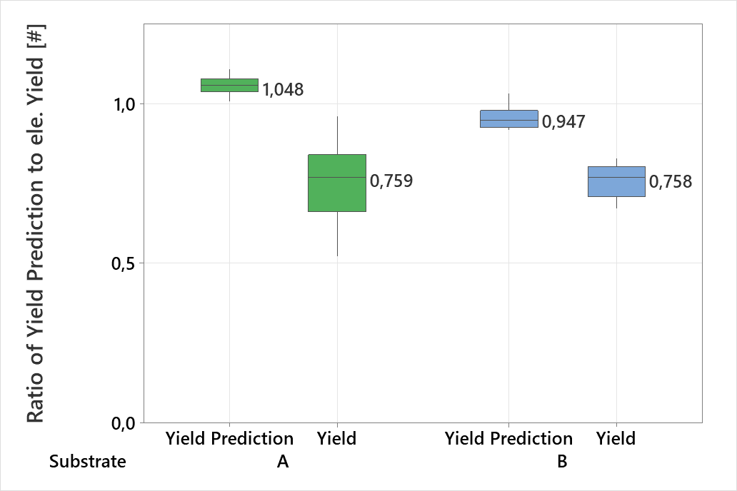
In Fig. 2 the exemplary normalized defect-based yield prediction and the normalized real electrical yield on wafer level tests of 23 wafers is shown. The average yield prediction was set to 1 and all other values were adjusted accordingly. The Trench-MOSFET devices were manufactured on substrates of two different suppliers (A and B). Fig. 2 shows that the accuracy of the defect-based yield prediction varies between different substrates. For substrates A the defect-based yield prediction is on average 1.048. For substrates B the average yield prediction is 0.947. The normalized electrical yield for substrates A is on average 0.759 and 0.758 for B. Furthermore, the average difference between defect-based and electrical device yield for substrates A is 0.289 and 0.189 for B.

Fig. 2. Normalized defect-based yield prediction vs. normalized electrical yield on wafer level tests of two substrate suppliers. For the defect-based yield prediction a device layout and only device critical defects were considered.
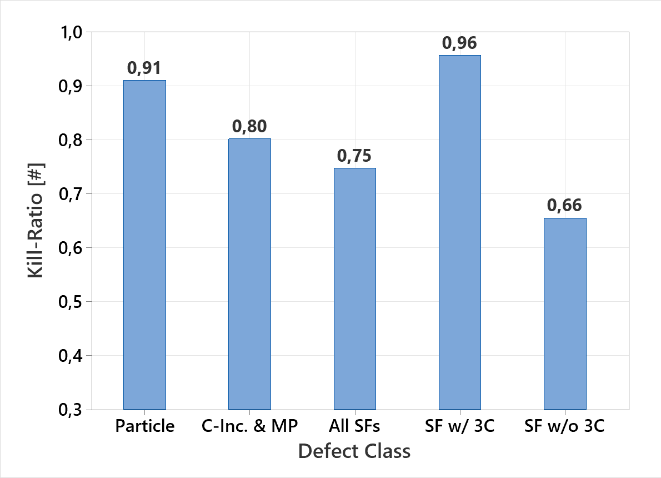
Fig. 3 shows the calculated KR for chosen critical defect classes of more than 500,000 TrenchMOSFETs on substrates B. The KR for particles and related defects is 0.91 and for C-inclusions and micro-pipes (MPs) 0.8. Considering all types of stacking faults (SFs) with a surface topology the KR is 0.75. Dividing all SFs into SFs with 3C-inclusions and into (partial) SFs without 3C-inclusions the KR is 0.96 and 0.66, respectively.

Fig. 3. Calculated “Kill-Ratio” of most important critical defects on more than 500,000 electrically analysed Trench-MOSFET devices on supplier B substrates.
Discussion
Comparing the normalized defect based predicted yield with the (wafer level) electrical yield of 23 different substrates (Fig. 2) shows a significant difference in prediction accuracy. For substrates of supplier A, a difference between normalized predicted and electrical yield of 0.289 and 0.189 for epitaxial layers on supplier B substrates is measured. Therefore, on supplier B substrates the yield prediction is more accurate by 0.1. All wafers have been processed with the same tools as well as under the same conditions as far as possible. Thus, an influence due to process variation during device production has been reduced as much as possible. It is possible that this difference is due to a reduced detection of device critical defects or because of substrate intrinsic variation, e.g., doping level and homogeneity or substrate defects. An improvement to the defect detection algorithm could increase the yield prediction accuracy on supplier A substrates because some extended defects, e.g., stacking faults, can differ slightly in their occurrence between A and B.
Conclusion
This paper shows the high accuracy of defect-based yield prediction that can be achieved for Trench-MOSFET devices regarding electrical yield on wafer level. Additionally, the “Kill-Ratio” of the most important device critical extended defect classes as well as the main failure mode of affected devices during electrical testing are discussed. Therefore, a total of around 1,000 substrates (supplier A and B) were characterized for their defects with the definite device layout. With those wafers more than 500,000 similar Trench-MOSFET devices have been manufactured using a typical process flow. Comparing the defect-based yield prediction with electrical yield for 23 wafers a clear difference in prediction accuracy was identified. The yield prediction is significantly more accurate on substrates of supplier B. The root cause for the difference between substrate suppliers (A and B) is still under investigation. Calculating the KR for devices on substrates B a correlation between the most important critical defect classes and device failure during wafer level tests was verified. Large defects, i.e., particle related defects, 3C-inclusions and MPs, and SFs with 3C-inclusions, resulted in an accurate defect-based prediction of electrical device failure. The KR of SFs without 3C-inclusions was lower due to the more varying occurrences of this type of defects. We were able to show that different leakage currents, i.e., 𝐼𝐼𝐷𝐷𝐷𝐷𝐷𝐷, 𝐼𝐼𝐺𝐺𝐺𝐺𝐺𝐺 and 𝑉𝑉(𝐵𝐵𝐵𝐵)𝐷𝐷𝐷𝐷𝐷𝐷, were the main electrical failure modes during wafer level tests for the most important extended defects. Most failure modes for devices affected by BPDs and scratches were identified to not correlate to leakage currents. BPDs are not known to affect the initial electrical device performance. Scratches need to be further differentiated into “shallow/deep” types for a more accurate defect-based yield prediction.
上一篇: 超声波水流清洗的最佳喷射距离