Abstract
Efficient and inexpensive photovoltaic systems are necessary to meet the increasing global electricity demand. In order to improve the efficiency of the crystalline silicon (c-Si) solar cells, the recombination losses of charge carriers must be reduced by the surface passivation techniques. Aluminium oxide (AlOx) thin films are highly relevant for various high efficiency silicon solar cells. In literature, AlOx layers are shown to be negatively charged dielectrics that provide an excellent passivation of lowly and highly doped p-type cSi surfaces. It is also shown in literature that high efficiency c-Si solar cells are passivated by AlOx films deposited using atomic layer deposition (ALD) and plasma-enhanced chemical vapour deposition (PECVD). Although several deposition techniques are mentioned in literature for AlOx deposition, solution processed AlOx thin film deposition technique is shown to be an inexpensive process. This thesis work aims to achieve excellent c-Si surface passivation by AlOx film using low cost deposition techniques. Two simple, inexpensive and non-vacuum deposition techniques — spin coating and spray coating — are investigated for surface passivation of p-type c-Si.
Introduction
According to the IERNA's new report, solar PV and wind are increasingly the cheapest renewable electricity sources in many markets around the world. A report by IEA indicates that solar PV is steadily cheaper than new coal- or gas-fired power plants in most of the world, and solar power projects now provide the cheapest electricity in history. According to IRENA, the global weighted average levelised cost of electricity (LCOE) generated from solar PV and onshore wind has fallen by 82% (United States dollar (USD) 68.4 per megawatt-hour (MWh)) and 45% (USD 52.8 per MWh) respectively over the period 2000–2019. IRENA expects that solar and wind power costs will continue to fall till 2030.
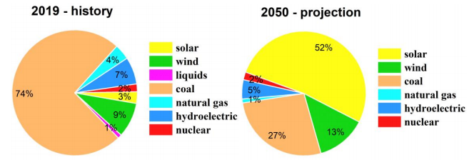
In India, solar is emerging as a major source of electricity surpassing other renewable technologies such as wind and hydro in future as shown in Figure 1.1. The electricity production from solar is expected to increase continuously and reaches 52% by 2050, from 3% in 2019.

Figure 1.1: Share of India’s electricity generation for selected energy sources by single region scenario, data adapted from
In general, the commercially available solar cell technologies can be classified into three major categories: wafer-based (mono-crystalline silicon and multi-crystalline silicon (mc-Si)), thin film technologies (copper indium selenium (CIS), copper indium gallium selenium (CIGS), cadmium telluride (CdTe) and organic PV) and multi-junction. A photovoltaics report said, “Si-wafer based PV technology accounted for about 95% of the total production in 2020. The share of mono-crystalline technology is now about 84% (compared to 66% in 2019) of total crystalline silicon (c-Si) production”. As reported in, the efficiencies of c-Si PV cells have reached above 25%. Although c-Si solar cells have higher efficiency, the cost of c-Si solar cells is high compared to mc-Si solar cells. The next challenge is reduction of c-Si solar cell cost and improving the performance by implementing enhanced solar cell concepts, materials and technologies compatible with mass production at low costs.
Surface Passivation of Silicon - a Literature Review
In order to develop solution processed AlOx film as a surface passivation layer, it is necessary to understand the physics of surface recombination and how it can be reduced using a passivation film such as AlOx. This chapter starts with a discussion of an industrial PERC solar cell structure. It discusses recombination mechanisms in semiconductors. A literature survey reviewing the surface passivation quality of various dielectrics such as silicon dioxide (SiO2), silicon nitride (SiNx), hydrogenated amorphous silicon (a-Si:H) and Al2O3 is presented. This section also presents a review of the experimental techniques reported in literature to deposit AlOx films such as ALD, PECVD, sputtering, spin coating and spray coating processes. A literature survey on surface preparation, effect of film thickness, optical properties requirements, activation of surface passivation, thermal stability, and passivation characteristics of AlOx/c-Si interface is presented. A literature survey on emitter passivation is also presented. It also includes review of crystalline silicon solar cells such as PERC, passivated emitter rear totally diffused (PERT), passivated emitter and rear locally diffused (PERL), tunnel oxide passivated contact (TOPCon) and interdigitated back-contact (IBC) cells. It also discusses integration of backside passivation layers in PERC solar cells.
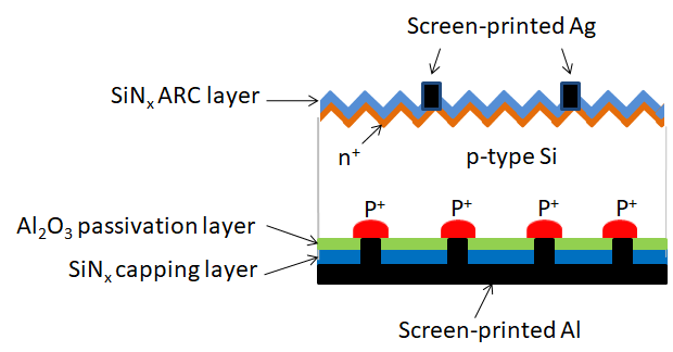
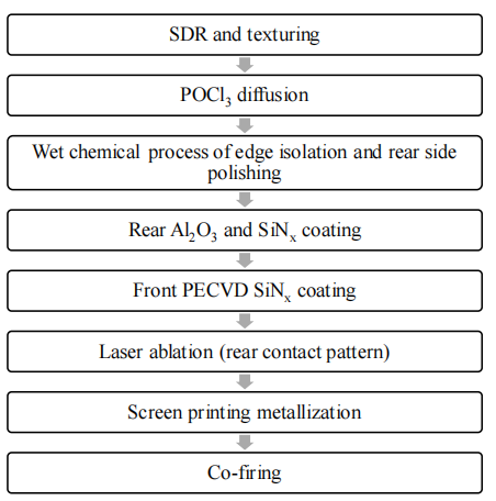
The structure and the corresponding process flow of an industrial type Al2O3 PERC cell are shown in Figure 2.1 and Figure 2.2, respectively. The process flow of a typical industrial PERC cell starts with p-type Czochralski (Cz) c-Si wafer. The wafers usually have surface damages due to saw cutting and saw damage removal (SDR) process is performed to remove the damaged regions. After SDR process, the wafer surface is textured chemically to reduce optical reflection from the silicon surface. Then, an n-type emitter layer is grown by thermal diffusion process using phosphorus oxychloride (POCl3) as dopant precursor. Edge isolation and rear side polishing is performed to remove electrical shorting between front and rear surfaces and to enhance light reflection from rear side, respectively. Al2O3 layer is deposited for rear surface passivation followed by deposition of SiNx as capping layer. A SiNx anti-reflection coating (ARC) layer is deposited on the front emitter layer for emitter passivation and light management. Laser is used to selectively remove Al2O3/SiNx layer from the rear side to form local back surface field (BSF) (p + ) during metallization. Finally, printing and co-firing is carried out for electrical contacts using silver (Ag) paste at the front side and aluminium (Al) paste at the rear side.

Figure 2.1: Schematic drawing of a typical industrial PERC solar cell structure

Figure 2.2: Process flow of CSUN’s industrial PERC solar cell
Surface passivation materials
High efficiency silicon solar cells strongly relay on surface passivation. The most important silicon surface passivation materials used for PV applications include SiO2, SiNx, aSi:H and Al2O3.
Silicon dioxide (SiO2)
Thermally grown SiO2 is one of the important and widely used materials for applications in silicon based microelectronics. In silicon photovoltaics, SiO2 is a very important material. The low interface state densities associated with the Si/SiO2 interface reduce the surface recombination significantly and have enabled high solar cell efficiencies. In literature, very low Dit of ~109 eV-1 ·cm-2 and positive Qf over a range of 1010 – 1012 cm-2 was reported.
In our work, AlOx films deposited by wet chemical processes are investigated for ptype c-Si surface passivation. The following aspects are investigated:
1.Synthesis of transparent and clear AlOx solution using aluminium nitrate nonahydrate precursor and 2-methoxy ethanol solvent by ultrasonic agitation at room temperature.
2.Deposition of AlOx films using prepared AlOx solution by spin coating and spray coating techniques—hand-held sprayer and spraying instrument—on silicon substrates.
3.Optimization of chuck design for spraying instrument using PL imaging.
4.Custom designed spraying instrument and hot plate heater with large area capabilities.
5.Implementation of ultrathin SiOx film grown by UV/O3 prior to AlOx spray coating by spraying instrument.
6.Investigation of physical, electrical and surface passivation properties of deposited AlOx films. Investigation of p+ emitter passivation by spray coated AlOx film.
7.Patterning of spray coated AlOx film by photolithography.
8.Laser fired contact process for making local rear contacts through spray coated AlOx film.
下一篇: 温度对弱配位溶剂中半导体电沉积的影响