ABSTRACT
Temperature is an important variable in electrochemistry, increasing the operating temperature has the capacity to provide significant increases in mass transport and electron transfer rates. In the case of electrodeposition, it can also allow the deposition of crystalline material which would otherwise be amorphous when grown at lower temperatures. In this work we exploit a high boiling point, weakly coordinating solvent, odichlorobenzene, to electrodeposit the p-block semiconductors antimony and antimony telluride at temperatures up to 140 °C. The effect of the temperature on the morphology and crystallinity of the deposits is investigated using scanning electron microscopy, X-ray diffraction, Raman spectroscopy and optical microscopy. An attempt is also made to rationalise the role of temperature in electrodeposition and its influence on the aforementioned properties.
1. Introduction
Weakly coordinating solvents (WCSs) are of interest for semiconductor electrodeposition because they are poor Lewis bases and so do not interact strongly with the metal precursor dissolved in solution. This is important in the electrodeposition of alloys and compounds because solvent interference can disrupt the speciation of the metal complex and cause variations in the deposition potential, electron transfer kinetics and mass transport of the metals. This can greatly complicate the process of achieving co-deposits with a controlled stoichiometry.
Recently, dichloromethane (CH2Cl2, DCM) has been used as a WCS to successfully electrodeposit various p-block metal semiconductors, such as Bi2Te3, HgTe , and Ge2Sb2Te5. However, DCM has a low boiling point and high volatility, which can make it practically challenging to use, and also restricts experiments to near room temperature. In a recent study, o-dichlorobenzene (oDCB) was identified as a promising WCS for the electrodeposition of semiconductors. oDCB was shown to behave electrochemically similarly to DCM, but with a boiling point of 180 °C, much greater than the 40 °C for DCM, therefore allowing the possibility of electrodeposition at elevated temperatures from a weakly coordinating solvent.
2. Experimental
2.1. Chemicals
o-dichlorobenzene, C6H4Cl2 (oDCB) (>99% Sigma-Aldrich, UK) was dried and degassed by refluxing with CaH2 under a dinitrogen atmosphere followed by distillation, and was stored in an ampoule under an inert atmosphere of N2. The water content in the solvent was measured with Karl–Fischer titration (KF 899 Coulometer Metrohm, UK), averaging less than 30 ppm across batches of solvent. Tetrabutylammonium chloride, [Nn Bu4]Cl (>99% Sigma-Aldrich, UK) was dried by heating at 100 °C under vacuum for several hours. Decamethylferrocene, [{C5(CH3)5}2Fe] (DMFc) (>97% SigmaAldrich, UK) was purified by sublimation. Tetrabutylammonium tetrachloroantimonate(III), [Nn Bu4][SbCl4] and tetrabutylammonium hexachlorotellurate(IV), [Nn Bu4]2[TeCl6] were prepared using methods previously described in the literature. Antimony(III) telluride lumps (99.999% Alfa Aesar, UK) for the EDX standard were used as received. All solvents and reagents were stored in a dry, N2 purged glovebox.
2.2. Electrodes
A Pt mesh was used as the counter electrode, the reference electrode was a custom made Ag/AgCl immersed in a storage solution of 100 mM [Nn Bu4]Cl, separated from the electrolyte by a porous glass frit. Substrates for electrodeposition were 20 × 10 mm thin film TiN on Si chips with a 4 mm diameter exposed area. The substrates were manufactured using typical microfabrication methods in a manner that has been described previously. Briefly, 200 nm thick layer TiN was plasma sputtered onto Si/SiO2 wafers followed by the sputtering of a 200 nm SiO2 layer. The top SiO2 layer was patterned by photolithography and half etched by plasma dry etching and removed completely using a buffered oxide etchant. A Cr/Au 10/190 nm layer was deposited via thermal evaporation onto the contact area to minimise contact resistance.
2.4. Electrochemical measurements
All glassware was cleaned by soaking in Decon 90 (Decon Laboratories Ltd., UK) for at least 24 h, followed by rinsing with ultrapure water, 0.055 µS cm−1 and then dried in an oven for a further 24 h. Experiments at elevated temperatures necessitated a novel cell design. The potential of the reference electrode is temperature sensitive and so a ‘non-isothermal’ cell was used based on an approach taken by Weaver, fabricated in the School of Chemistry glass workshop at the University of Southampton. In this design the cell is composed of two compartments, one containing the WE and the CE that is heated, and a separate compartment housing the RE that remains at room temperature. A schematic is given in the SI. The main compartment was jacketed with silicone oil (Alfa Aesar, UK). Heat was provided by a RCT digital hot plate (IKA, UK) with the temperature in the cell controlled with a PT1000.90 temperature sensor (IKA, UK). The WE and CE were fed through GL14 ports, and sealed with silicone rubber sealing rings with a PTFE washer (DWK Life Sciences, Germany) held in place with apertured PBT screw caps (DWK Life Sciences, Germany). The electrolyte was prepared in a glovebox (Belle Technology, UK) under an inert atmosphere of N2 in the presence of <5 ppm O2 and H2O. The cell was then loaded, sealed, removed from the glovebox and connected to an Ar gas line, with a gas bubbler fitted to the cell. Ar was flowed whilst heating to maintain an inert atmosphere, and then switched off during experiments. Measurements were performed with a PGSTAT µIII (Metrohm Autolab, UK) potentiostat. Data was recorded with NOVA 1.11 (Metrohm Autolab, UK).
3. Results and discussion
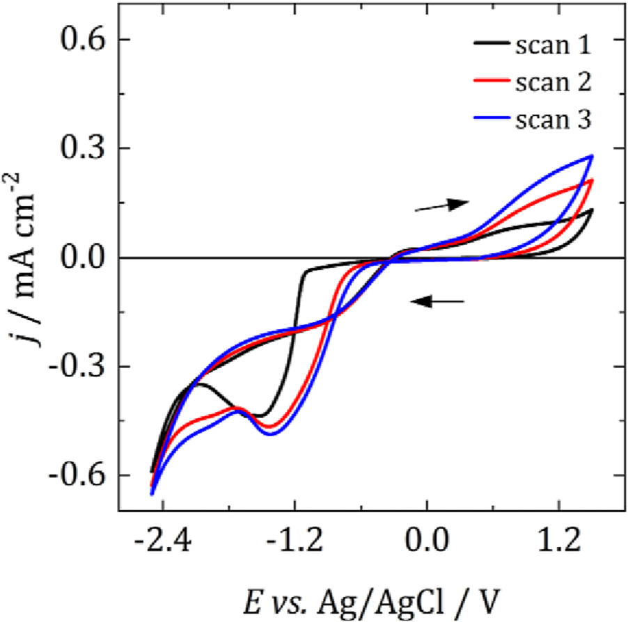
Fig. 2 shows a voltammogram of 3 mM [Nn Bu4][SbCl4] at a TiN electrode at 25 °C. Scanning negatively, a reduction current is observed, beginning at approx. −1.2 V vs. Ag/AgCl which can be attributed to the electrodeposition of Sb. This results in a peak at ca. −1.6 V, followed by the onset of electrolyte breakdown at −2 V. On the return scan the current crosses the x-axis at −0.5 V and a small amount of stripping occurs. There are no major changes to the voltammetry on subsequent scans.

Fig. 2. Voltammograms of 3 mM [Nn Bu4][SbCl4] and 100 mM [Nn Bu4]Cl at a 4 mm dia. TiN WE in oDCB at 25 °C. Scan swept from 0.5 V vs. Ag/AgCl at 100 mV s−1 in the direction indicated by the arrows. CE: Pt mesh, RE: Ag/ AgCl.
Depositions were performed at −1.8 V, corresponding approximately to the peak in the voltammogram above. Depositions were performed with a cut-off charge, which corresponded to the charge passed after a 30 min deposition at 25 °C. A voltammogram of [Nn Bu4][SbCl4] was also recorded at 100 °C (see Fig. S3) to assess any changes in the crossover potential for Sb deposition and stripping. The potential shifted by less than 100 mV, and so it can be assumed that the overpotential for deposition remained constant with temperature.
SEM images of the deposits collected at each temperature are shown in Fig. 3. At 25 °C, the deposits grow as a compact film with clumps of Sb dispersed over the surface. As the temperature increases, the film becomes smooth and homogeneous. Finally at 140 °C, Sb grows primarily as small islands on top of the electrode. This therefore shows a significant improvement in the quality of the morphology of the film, simply by increasing the deposition temperature and without the need for additives.

Fig. 3. SEM images of Sb deposited at varying temperatures onto a TiN substrate from oDCB containing 3 mM [Nn Bu4][SbCl4]. Scale bar represents 10 µm.
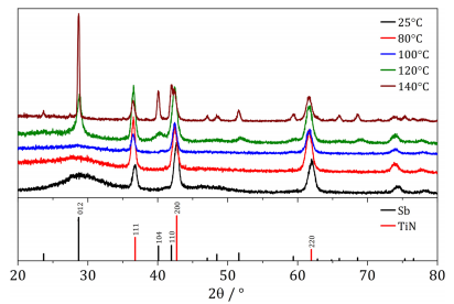
Fig. 4 shows XRD patterns from the Sb deposited at each temperature. At 25 °C a single broad peak associated with the deposit can be observed at ca. 28°, which corresponds to the primary diffraction peak of elemental Sb. The calculated lattice parameters in Table 2 show good agreement with the literature values for Sb. The shape of the peak suggests that the material is amorphous, as reported by Reeves et al. when deposited from DCM. This is also indicated by the small average crystallite size estimated from the Scherrer equation, also in Table 2. Up to 100 °C the XRD pattern does not change significantly with increasing temperature, suggesting that whilst the morphology of the deposit is changing, the temperature is having a negligible effect on the crystallinity of the deposited Sb. This is also reflected in the average crystallite sizes, which remain effectively constant. At 120 °C however, a defined peak at 28° appears, and minor diffraction peaks of Sb can also be observed. Then upon heating to 140 °C a far more intense peak occurs, and the large crystallite sizes indicate that Sb was deposited in a crystalline form.

Fig. 4. XRD patterns of Sb electrodeposited on TiN at varying temperatures from oDCB containing 3 mM [Nn Bu4][SbCl4]. Black: 25 °C, red: 80 °C, blue: 100 °C, green: 120 °C, brown: 140 °C. Bottom panel shows in black the literature pattern for Sb (ICSD 64695), and in red TiN (ICSD 152807). Offset is arbitrary and added for clarity. (For interpretation of the references to colour in this figure legend, the reader is referred to the web version of this article.)
4. Conclusions
oDCB was used to study the effect of temperature on the electrodeposition of antimony and antimony telluride. SEM images indicated that the deposits became smoother and more homogeneous as the temperature increased. Deposition at higher temperatures also improved the crystallinity of the resulting deposits, as evidenced by XRD analysis.
The antimony content in antimony telluride co-deposits decreased with increasing temperature, and it was no longer possible to electrodeposit stoichiometric Sb2Te3. This was attributed to changes in the relative affinity of freshly reduced Sb and Te atoms for themselves or the complementary metal in the alloy with temperature. Since the electrolyte remains unaffected by temperature up to 120 °C, in principle it will be possible in the future to optimise the ratio of the precursor concentrations for a given temperature. This will permit the electrodeposition of stoichiometric material with the additional bene- fits of using elevated temperatures.
Finally, for a given material it remains unclear on a microscopic level why exactly increasing the operating temperature causes a change from deposition of amorphous materials to crystalline materials and over what temperature range this transition will take place. There does not appear to be a satisfactory explanation for this phenomenon in the literature. It may, however, be possible to gain insight from knowledge on the mechanisms of crystallisation. Here, the transition from amorphous to crystalline is treated as a thermally-activated process, meaning the rate of crystallisation follows an Arrhenius type relationship with an associated activation energy of crystallisation. Therefore when the bath temperature is increased, a greater proportion of the reduced atoms are able to overcome the activation energy of crystallisation and so the deposit adopts a crystalline form.