ABSTRACT
This review paper gives an overview of recent developments in nanoparticle research and semiconductor industry applications. Nanoparticles have become useful building blocks for a variety of semiconductor devices and processes. Quantum dot technology, thin-film deposition, chemical mechanical planarization, and semiconductor nanocrystals are some of the main fields where nanoparticles have made significant strides. It highlights the special traits and skills of nanoparticles that allow for novel functionalities and enhanced efficiency in semiconductors. Nanoparticles are extremely important in the production of semiconductors because of their special characteristics and uses such as copper, gold, silver, etc. These nanoparticles are crucial for developing semiconductor technology because they provide improved thermal stability, increased conductivity, and compatibility with current fabrication methods. Their incorporation into semiconductor manufacturing procedures aids in the creation of high-performance hardware, and the execution of novel applications. This review paper also recognizes the difficulties in synthesizing, integrating, and taking safety precautions with nanoparticles. This paper emphasizes the need for more research and development to get around current obstacles and guarantee their successful implementation while recognizing the promising role that nanoparticles will play in determining the future of semiconductor applications.
1. Introduction
At the nanoscale, which pertains to the atomic or molecular level, materials are purposefully designed and engineered in the realm of nanotechnology. This field allows for the development of innovative materials, tools, and systems that exhibit enhanced capabilities due to their manipulation of structures and particles at an extremely minute scale. A nanoparticle is defined as a structure that experiences confinement in all three dimensions: x, y, and z. Conversely, when a structure is confined to only two dimensions, it takes the form of a nanowire or nanorod. Although a thin film has the ability to stretch over long distances in the x and y directions, its confinement remains limited to the z-direction. When it comes to analysis and characterization, particles are commonly treated as spheres or rods, despite their crystalline structure often leading to multifaceted shapes. Classification of structures can be based on the number of dimensions in which their size is restricted. It could revolutionize a number of fields, including environmental science, electronics, medicine, and energy, providing answers to urgent problems and creating new opportunities for scientific research and technological development.
Semiconductors are substances with characteristics halfway between conductivity and insulativity. As the basis for semiconductor devices like transistors, diodes, and integrated circuits, they are essential to modern electronics. Semiconductors are crucial for the manipulation and processing of information in electronic devices because they have the capacity to control the flow of electrical current. The electrical conductivity of semiconductors can be changed by doping them with impurities, which enables the development of sophisticated electronic components that power the modern digital world we live in Ref.. Table 1 presents a summary of the characteristics exhibited by semiconductors.
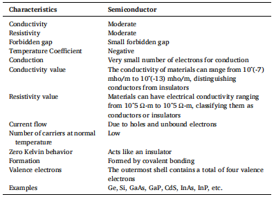
Table 1 Material properties of semiconductors
The goal of this review paper is to provide an overview of recent advancements in nanoparticle research and their applications in the semiconductor industry. The first part highlights the significance of nanoparticles as building blocks in various semiconductor devices and processes. The second part emphasizes the unique properties of nanoparticles that enable the introduction of novel functionalities and improved efficiency in semiconductors applications. The third part discussed the manufacturing processes of semiconductors in industrial level. The fourth and fifth parts analyzed NPs uses in semiconductors and semiconductors productions respectively. In final part, this paper acknowledges the challenges in synthesizing, integrating, and ensuring safety with nanoparticles. In conclusion, we need further research and development to overcome these obstacles and ensure successful implementation, recognizing the promising role of nanoparticles to shape the future of semiconductors applications.
2. Importance of semiconductor
Gadgets such as mobile phones, radios, televisions, computers, video games, and medical diagnostic apparatus, which are a vital aspect of our lives, rely on semiconductors for their functioning. Without semiconductors, these electronic devices would not be possible. Semiconductor lasers with delayed feedback have proven to be well-suited for solving challenging and time-consuming tasks in photonic reservoir computing. In this technique, the reservoir is frequently optically injected with the input data. Semiconductor helps electronics work by controlling the flow of electricity. In telecommunications equipment and systems, network and communication chips are semiconductor integrated circuits (IC). A variety of technologies are utilized in networking and communications chips, with a semiconductor material serving as the vital link between the conductor and the insulator. This material plays a crucial role in controlling and directing the flow of electricity within electronic devices and equipment. Consequently, it finds extensive application in electronic chips used for solid-state storage, computing components, and various other electronic devices. As AI and machine learning enter and develop inside the banking industry, semiconductor chips assist banks even more. This wasn’t a primary concern in the past because most attacks used software that was vulnerable to remote hacking.
An LED, an acronym for light-emitting diode, operates as a semiconductor that facilitates the flow of electric current in a single direction. It is designed as a p-n junction diode, as depicted in Fig. 1, with an abundance of electrons residing in the n-type atoms and electron holes present in the p-type atoms. When an electric current is applied, it pushes the atoms towards the junction, causing the n-type and p-type atoms to come close together. Consequently, the excess electrons from the n-type atoms are transferred or “donated” to the p-type atoms, resulting in the accumulation of negative charge on the n-side. This accumulation initiates a current that moves from the negatively charged region to the positively charged region, known as “forward bias.” At the same time, as the extra electrons from the n-type material pass through the holes in the p-type material, they release energy in the form of light, known as photons. LEDs demonstrate significant distinctions when compared to conventional light sources such a lamps, neon lamps, and gas discharge lamps. They possess the ability to illuminate swiftly, making them advantageous for battery-operated or energy-efficient devices. Moreover, LEDs generate a greater amount of light per Watt in comparison to incandescent bulbs (see Fig. 2).
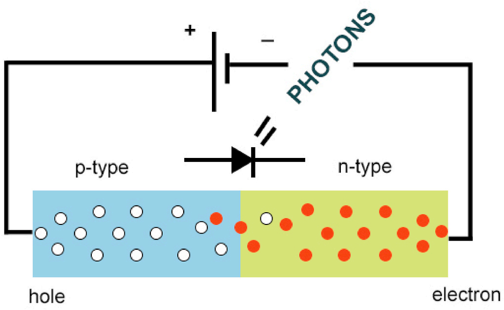
Fig. 1. A circuit diagram of semiconductor chip
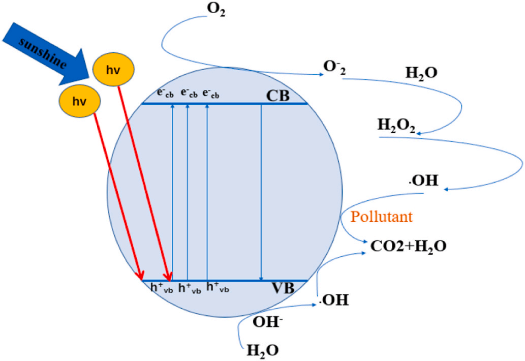
Fig. 2. Photocatalytic reaction mechanism
4. Semiconductor manufacturing process
One of the biggest industries in the world now is the electronics sector. The production of integrated circuits is a crucial component of this sector. On silicon wafers, integrated circuits are manufactured in the semiconductor industry. Historically, cost-cutting measures have included shrinking chip size, expanding wafer size, and raising yield while also attempting to enhance operating procedures inside semiconductor manufacturing systems . Integrated circuit (IC) usage has been rising quickly and will probably keep doing so in the near future. As a result, the production of semiconductors remains a hot topic in the world of manufacturing.
Wafer lithography
A lithographymethod for processing a semiconductor wafer is provided. The method involves the following steps: extracting liquid from the wafer’s surface, eliminating a part of the oxide film from the wafer’s surface, and introducing an oxidizing gas. Notably, the oxidizing gas flow and/or the surrounding gas affected by the oxidizing gas possess an unsaturated vapor pressure of the liquid, resulting in the vaporization of the liquid present on the surface. The creation of wafers, which are mostly constructed from silicon substrates, is the first step in the fabrication of semiconductors. The successful creation of VLSI products, particularly processor chips, relies heavily on the impeccable chemical purity and nearly flawless crystalline characteristics of wafers. The production of silicon wafers involves a multitude of intricate stages, such as refining raw materials, growing silicon ingots, peripheral grinding, slicing the ingots into wafers, beveling, lapping and etching, heat treatment, polishing, thorough cleaning with ultra-pure water, inspection, packaging, and finally, shipping. As a result, the entire process has become progressively more intricate and sophisticated. The general semiconductor wafer fabrication process flow is depicted in Fig. 3 . Once the wafer fabrication process is complete, the wafers undergo a probe test to examine their electrical distributions and yield before being forwarded for assembly and final testing (see Fig. 4).
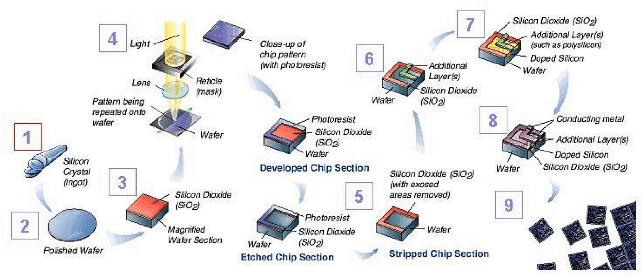
Fig. 3. Process flow for semiconductor wafer fabrication
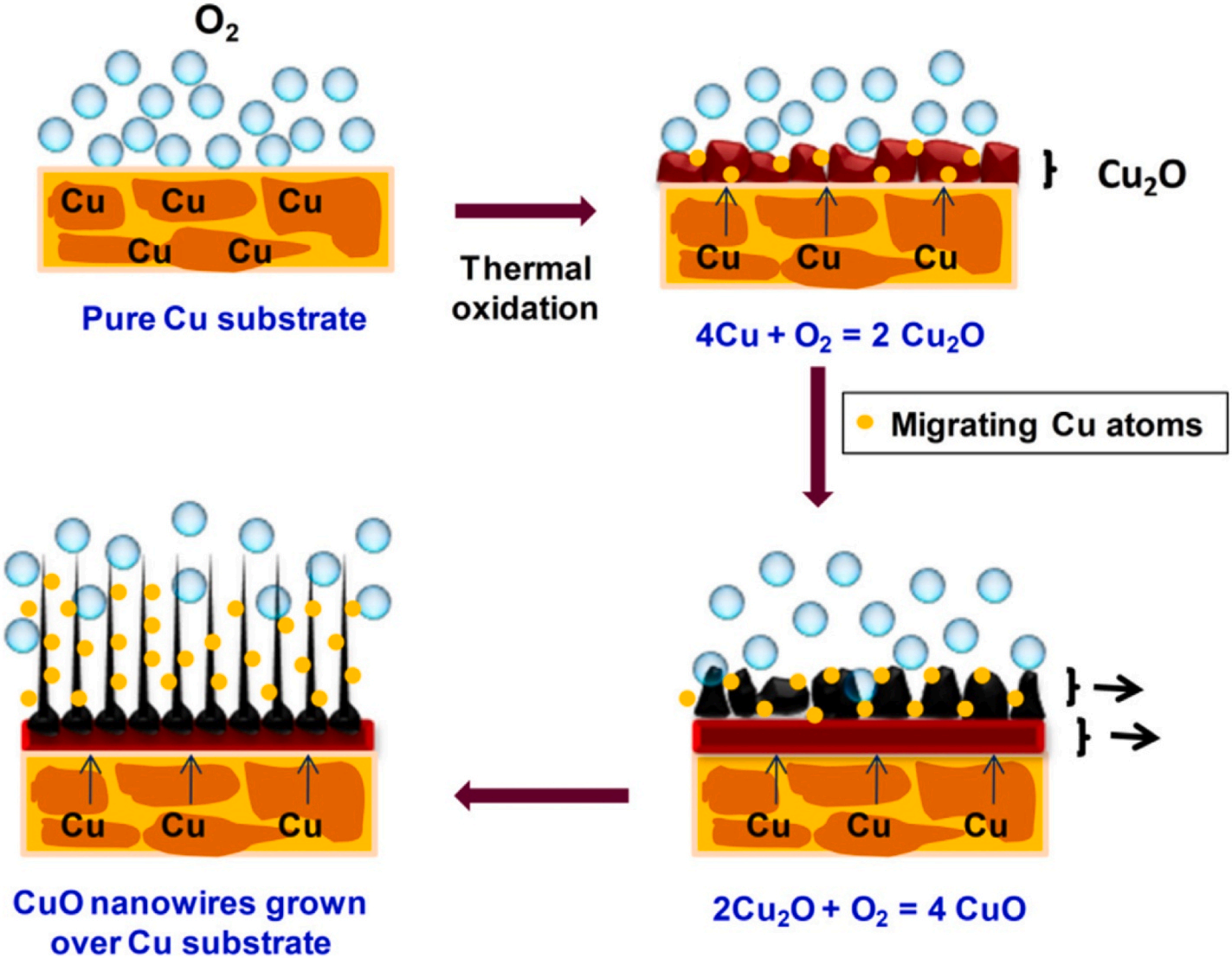
Fig. 4. Cupric Oxide nanowires form on a Cu substrate via thermal oxidation and this growth can be depicted schematically
Etching
Etching, a critically important step, is involved in the removal of material and plays a vital role in the overall manufacturing process (see Fig. 5) . A highly regulated layer-by-layer material removal procedure is called atomic layer etching. The semiconductor industry has been fabricating electronic circuits since the 1970s using a pattern-transfer methodology that is very similar to the early art form. The patterns are only now 100,000 times smaller thanks to a wafer fab equipment market worth well over $40 billion annually. With today’s technology, we may deposit different thin films in place of beeswax, use ultraviolet light to print patterns rather than needles that can be held in the hand, and use plasma to etch into the target material as opposed to an acid bath. With modern plasma sources and control systems, plasma etch has improved greatly during the last 40 years.
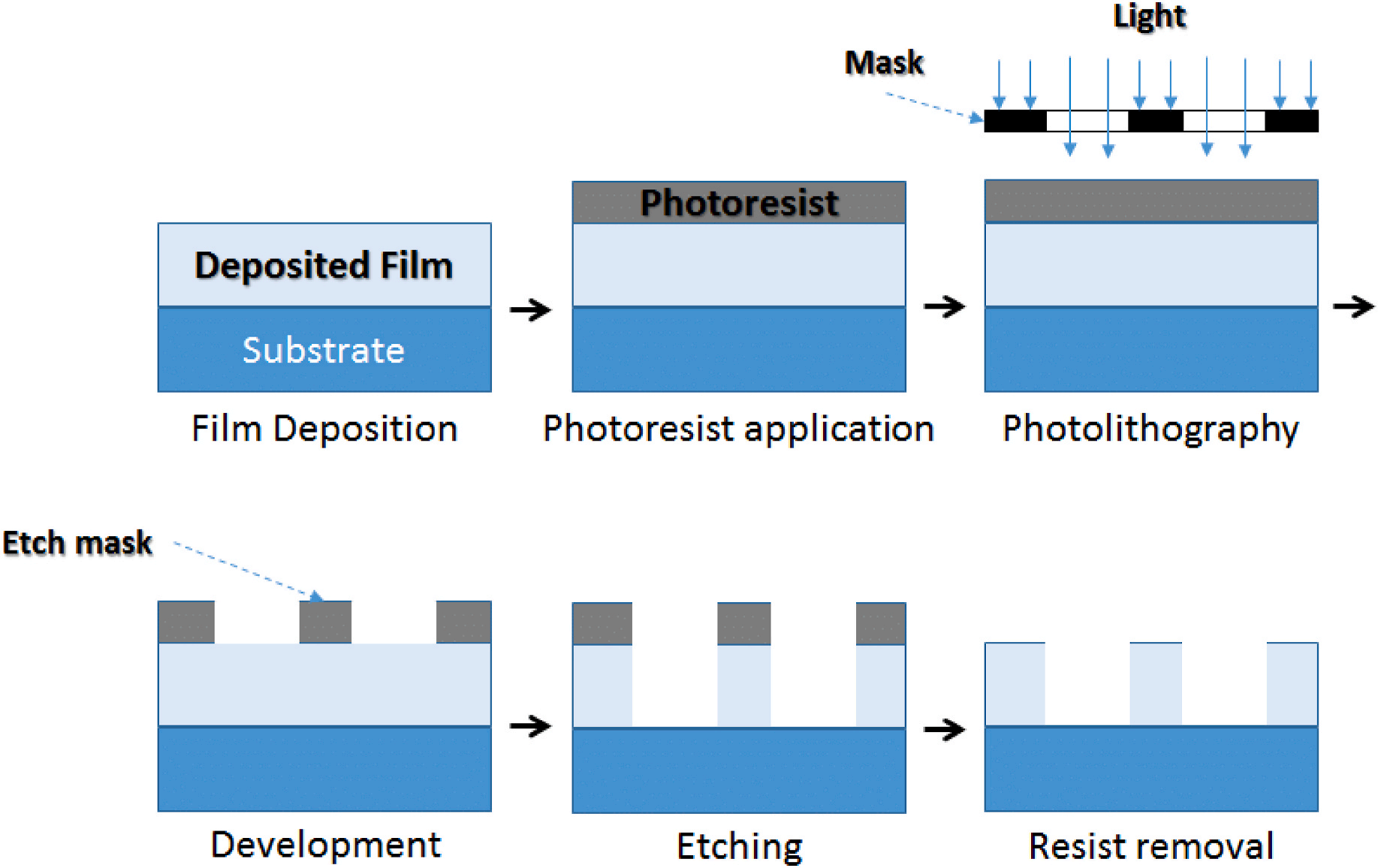
Fig. 5. The etching process for wafer fabrication
5. Conclusion
The use of nanoparticles in semiconductor applications has advanced the field significantly and created new opportunities. With their ability to enable precise control and improved performance, nanoparticles have proven valuable in a number of crucial processes, including chemical mechanical planarization, thin-film deposition, and semiconductor nanocrystals. With their tunable bandgaps and size-dependent emission, quantum dots have completely changed optoelectronic devices and display technologies. To fully realize the potential of nanoparticles in semiconductors, however, issues like synthesis control, integration, dependability, and safety must be resolved. In order to overcome these difficulties and guarantee the successful incorporation of nanoparticles into upcoming semiconductor technologies, ongoing research and development efforts are essential. The continued development and application of nanoparticles in semiconductor applications holds great promise for the future, spurring innovation and reshaping the electronic industry.
上一篇: 温度对弱配位溶剂中半导体电沉积的影响
下一篇: 硅半导体的光辅助电化学锂化