Highly aligned aggregation state structures have great significance for effective charge-carrier transport in organic semiconductors. Several methods have been developed to provide organic semiconducting molecules with highly oriented aggregation state structure; among these, using a water surface to form organic semiconductor films is a widely implemented strategy, wherein solutions are spread on the surface of water. However, common techniques of film formation on water surfaces generally result in a nonuniform orientation of the film owing to the isotropic spread process of droplets on the water surface. In this study, a spatially confined air/water interfacial assembly method is proposed to obtain uniformly aligned monolayer and multilayer poly(diketopyrrolopyrrole-thieno thiophene) thin films with controlled thickness. The structural and morphological characterizations obtained using atomic force microscopy, high-resolution transmission electron microscopy, and grazing incidence wide-angle X-ray scattering indicates the crystalline structure of the thin films and high alignment of the molecular chains. The maximum mobility of the thin films reaches up to 2.06 and 0.5 cm2 V−1 s−1 in the parallel and perpendicular direction, respectively, indicating apparent anisotropic electrical properties. Furthermore, an inverter based on these thin films exhibits a voltage gain of up to 70, demonstrating the potential of applying the proposed technique to logic circuits.
1. Introduction
The vigorous development of organic electronics has benefited from continuous improvement of the performance of organic semiconductors.Recently, the carrier mobility of organic semiconductors has been significantly improved, surpassing that of amorphous silicon.According to the chemical structures, organic semiconductors can be divided into small-molecule and polymeric semiconductors. Among them, polymeric semiconductors have attracted considerable attention owing to their stretchability and adequate solution processability.The mobility values range from ≈10−5 to 10 cm2 V−1 s−1 with the development of new materials and the application of novel technologies. Consequently, these semiconductors have broad application prospects in flexible electronic devices. Organic field-effect transistors (OFETs) are core components in organic electronics, which form the basis for organic circuit systems to perform various functions. Polymeric semiconductors are commonly used as conducting channel materials in thin films OFETs to fabricate high-performance and stretchable transistor devices. The electrical properties of polymeric semiconductors are significantly affected by their molecular and crystalline multi-level structures. Theoretically, the chargecarrier can transport rapidly along the main straight chain of the polymer, and the mobility can exceed 102 cm2 V−1 s−1 . However, in actual OFETs, the charge-carrier mobility of the polymeric semiconductor is considerably lower than the theoretical value. In addition to the impact of defects in the chemical structure of organic semiconductors, such as oxidized sites and poor planarity, certain drawbacks of polymeric semiconductor films fabricated using traditional methods, such as the large bends of chains, charge-carrier traps in the films, packing model of chains and boundary between crystalline/amorphous regions, hinder the effective charge carrier transport.Therefore, a simple and effective strategy is required for controlling the orientation of polymer molecular chains to achieve efficient charge-carrier transport and improve device performance.
2. Results and Discussion
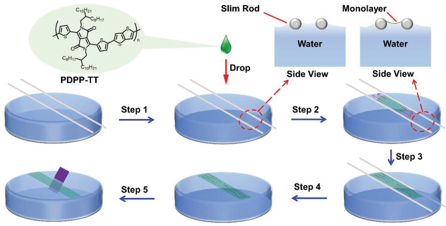
Two slim rods were used to form the spatially confined air/ water interface, and a narrow-confined area on the water surface was obtained. As shown in Figure 1, ultrapure water was poured into a clean Petri dish until the water level was slightly above the edge. Due to the surface tension of water, the upper surface of the water exhibited slightly upward convexity without overflow. Two slim rods were placed parallel on the Petri dish and embedded at the air/water interface to form a pair of long sides of a confined rectangular area. PDPP-TT was used as the semiconductor, which was dissolved into chlorobenzene to form a solution with a concentration of 0.5 mg mL−1 . During the assembly process at the air/water interface, 2.5 µL of 0.5 mg mL−1 PDPP-TT chlorobenzene solution was dropped at the center of the confined area. The semiconductor solution spread rapidly on the water surface. A high-speed video (Video S1, Supporting Information) was recorded to observe this rapid spreading process. Figures S1–S3, Supporting Information, illustrate a set of comparison photos and schematics of the air/water interfacial assembly method and the confined interface coating process. Owing to the existence of slim rods, the solution was hindered along the short-side direction of the rectangular confined area and rapidly spread only along the long-side direction to generate thin films.

Figure 1. Schematic diagram of air/water confined interfacial assembly method of polymeric semiconductor poly(diketopyrrolopyrrole-thieno[3,2-b] thiophene) (PDPP-TT).
The spreading of semiconductor solution at air/water interface can be explained by the Marangoni effect, which is caused by surface tension gradient at the two-phase interface. As the surface tension of water and chlorobenzene at 25 °C are 71.99 mN m−1 and 32.42 mN m−1 , respectively, the PDPP-TT solution can spread rapidly on water surface during the air/ water interfacial assembly process. Marangoni flows are known to spread only for a finite radius on nonconfined water surface because of critical micelle concentration.Following the fast Marangoni flows, there are secondary flows that are slow and unstable and the spreading radius are comparable with primary Marangoni flows, which is the crucial stage that confined process works. During the assembly process at the confined interface, the existence of slim rods limited the plumbing instability of the secondary flows. Consequently, the distance of spreading get much larger than Marangoni flows radius because the inertia of boundary layer and its slow diffusion makes the spreading of Marangoni flow get into an inertial jet. In other words, the lateral confinement of the flow can change the extent of these inertial secondary flows and form an inertial surface jet to spread to larger distances in the longaxis direction. In this case, the films obtained by the spatially confined air/water interfacial assembly method had a larger diffusion distance than Marangoni radius and the continuous inertial action made polymer chains highly aligned during the jet quickly spreading process.

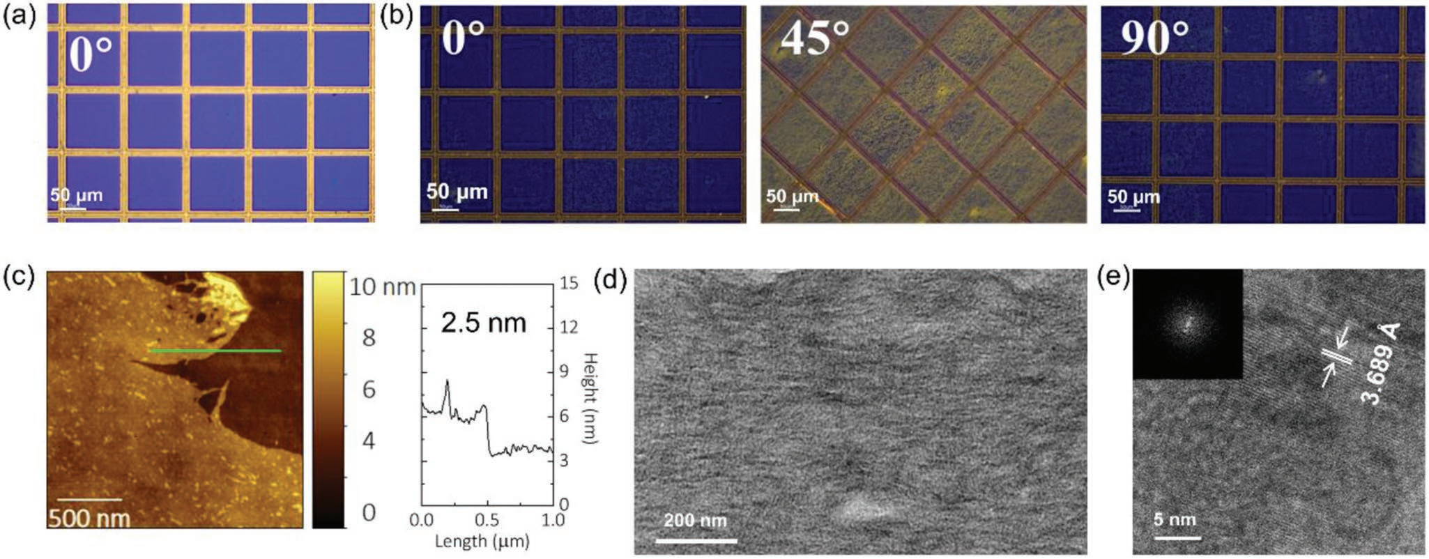
Figure 2. a) Optical microscope (OM) and b) polarized OM images of thin films obtained using the spatially confined air/water interfacial assembly method at different rotation angles. c) Atomic force microscopy image and sectional profile, d) Transmission electron microscopy (TEM) image, and e) high-resolution TEM (HRTEM) image of thin films obtained using the developed assembly method. The spacing distance of lattice fringes of π–π stacking in (e) is 3.689 Å, and the inset in (e) present the fast Fourier transform result of HRTEM stripes.
After the film was completely formed, the slim rods were carefully removed, and the obtained films can be transferred onto any substrate. Figure 2a,b show the optical microscope (OM) and polarize OM (POM) images of PDPP-TT monolayer films obtained using the spatially confined air/water interfacial assembly method. As the monolayer film was too thin to be observed on the Si/SiO2 substrate background, a copper mesh was covering as a reference. As shown in Figure 2a, the film was nearly transparent in the OM imaging mode because of its low thickness and only the Si/SiO2 substrate could be intuitively observed. When using the POM imaging mode and rotating from 0° to 45°, the film exhibited an obvious color change from dark to pale-yellow. The obtained image color returned to the dark shade when the film rotated from 45° to 90° (Figure 2b). This process verified the existence of the thin film and validated its molecular alignment and crystalline characteristics. Interestingly, certain highly aligned textures were observed in the POM image of the 45° rotation, exhibiting a wide range of consistent alignment of films obtained based on the spatially confined air/water interfacial assembly method.
To further investigate the structure and morphology of the thin films, polarized ultraviolet–visible–near-infrared (UV–Vis– NIR) absorption spectra were separately obtained for the films produced using spatially confined and nonconfined processes. As shown in Figure 3a,b, both films exhibited broad absorption from 600 to 900 nm, and the maximum absorption peak appeared at ≈800 nm. The film fabricated by the confined interface in the parallel direction exhibited two strong absorption peaks at 750 and 830 nm which were much more obvious compared to the vertical direction (Figure 3a), and the dichroic ratio is 2.1. Conversely, the films obtained using the nonconfined air/water interfacial assembly method exhibited no apparent difference in the two orthogonal directions (Figure 3b), and the dichroic ratio was close to that of spin-coated films.These results clarified that the highly aligned polymer chains were formed in the film when the spatially confined air/water interfacial assembly method was used. Furthermore, grazing incidence wide angle X-ray scattering (GIWAXS) measurements were characterized to analyze the molecular packing in thin films and monolayer films obtained using the spatially confined air/water interfacial assembly method. As illustrated in Figure 3c–e, three-layer, eight-layer, and spin-coated films exhibited similar GIWAXS signals. The four clear signals of out-of-plane (h00) signals were attributed to lamellar stacking of PDPP-TT chains, and the in-plane peak (010) at 1.79 Å−1 was attributed to π−π stacking of PDPP-TT. It can be obtained that PDPP-TT backbones in the thin films obtained using the spatially confined air/water interfacial assembly method take an edge-on orientation, which facilitates the transport of chargecarriers, particularly in 2D conducting networks. The different layers of films exhibited similar GIWAXS signals, indicating the uniformity of films and polymer chains stacking. However, the monolayer film was extremely thin to obtain identifiable GIWAXS signals. As an alternative, the monolayer sample was characterized by HRTEM. Figure 2e shows highly clear HRTEM lattice fringes, and 3.689 Å spacing concurred with the GIWAXS results. The Q-space signal of π−π stacking at 1.79 Å−1 (Figure 3d and Figure S6, Supporting Information) was close to the data of PDPP-TT π−π stacking distance. The HRTEM results provided direct evidence of highly aligned crystalline chains in the monolayer films of PDPP-TT obtained using the spatially confined air/water interfacial assembly method.
3. Conclusion
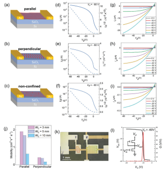
In this study, a spatially confined air/water interfacial assembly method was proposed to optimize the general air/water interfacial assembly method, resulting in uniform and highly aligned PDPP-TT films. The monolayer of PDPP-TT film was 2.5 nm thick, and the layer can be controlled by changing volume of the dropped solution. This implied that the thin films can be fabricated from monolayer to any needed thickness. The polarized UV-Vis-NIR absorption spectra indicated an anisotropic aggregation state structure in the films. Additionally, the carrier mobility of OFETs devices based on PDPP-TT thin films shows obvious anisotropy, which was consistent with the polarized UV-Vis-NIR absorption spectra dichotomous results. The impact of confined width on mobility was also analyzed, and the highest mobility of 2.06 cm2V−1 s−1 was achieved when the confined width was 3 mm for 2.5 µL PDPP-TT solution with a concentration of 0.5 mg mL−1 . An inverter circuit with a voltage gain of 70 was fabricated using the obtained thin films. The results verify the effectiveness of confined area for improving orientation and performance of films with air/water interface coatings. This method can serve as an efficient strategy for fabricating highly aligned polymer films, providing a new reference for the preparation of high-performance organic electronic devices.
4. Experimental Section
Materials: The semiconducting polymer PDPP-TT was synthesized by using a previously reported method,and P(NDI2OD-T2) was also synthesized according to the previously reported procedures.
Highly Aligned Monolayer Films Fabrication: A clean petri dish was filled with ultrapure water. Due to the surface tension of the water, the water surface was maintained slightly higher than the edge of the Petri dish without overflowing. Two clean slim rods were placed above the water surface and fixed to the edge of the Petri dish with tape at a set distance. The PDPP-TT solution was prepared as a concentrate of 0.5 mg mL−1 with chlorobenzene as the solvent. During the fabrication process of the highly aligned monolayer films, a drop of 2.5 µL PDPP-TT solution was dropped at the center of the confined air/water interface. The droplet rapidly spread to both sides after making contact with the water surface, forming a thin film oriented along the direction of the spreading motion at the air/water surface. The thin films with thicknesses of twoand three-layers were prepared by controlling the volume of the same concentration PDPP-TT solution with 5 µL and 7.5 µL. The thickness cannot be controlled by volume of the solution for films thicker than three layers, and the thicker films were obtained by stacking one to three layers thin films.

Figure 4. Schematics of organic field-effect transistors (OFETs) based on thin films obtained using the a) spatially confined air/water interfacial assembly method in the parallel direction, b) spatially confined method in the perpendicular direction, and c) nonconfined assembly method. d–f) Transfer curves and g–i) output curves of corresponding OFETs. j) Statistics and comparison of electrical performance with different confined widths in both parallel and perpendicular directions. k) Optical microscope image of an inverter based on the thin films obtained using the spatially confined air/water interfacial assembly method. l) Static switching characteristic of the inverter, the inset depicts the corresponding circuit diagram.
上一篇: 硅半导体的光辅助电化学锂化