Abstract
The evaluation of photovoltaic man-ufacturing wet process steps shows howimpurities may be deposited on siliconmedia. Upon withdrawing a wafer, a liguid layer remains on the silicon surface.Any contaminants in the liguid will bedeposited on the silicon when the liquidevaporates. This data shows the biggestfactor affecting deposition of impuritiesis the concentration ofimpurities in thebath.
The introduction of contaminants onsilicon media during processing canreduce the efficiency of ph otovoltaic (PV)cells and shorten their lifetime,One of thesources of contamination is processbaths, where media is dipped into waterand/or chemicals for etching or cleaning.The sources of bath contaminants arenumerus, They can arise from insuffi.ciently pure chemicals or water. Thetanks, silicon carriers and handlingequipment may be constructed fromindustrial-grade materials that desorbimpurities, thereby contaminating ba ths.Alternatively,the impurities could beextracted from common plastics used inindustrial-grade plumbing com ponents orchem ical containers.
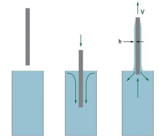
The folowing information discussesan examination of how a contaminatedprocess bath may potentially depositimpurities on silicon media, Upon with.drawing a silicon wafer from a bath, athin layer of liguid is left on the surface ofthe silicon, as depicted in Figure 1. Anycontaminants in the liguid layer will bedeposited on the silicon when the liquidevaporates, This infomation will showthat the biggest factor affecting deposi-tion of impurities is the concentration ofimpurities in the bath. Other factors suchas removal speed of the wafers from thebath and properties of the liquid includ.ing surface tension, density and viscosityare less influential.

Figure1-WaferSubmersion and Withdrawal From a Process Bath
Sources of Contaminationin Wet Processing
Processing of silicon wafers into pho-tovoltaic cells involves multiple steps.Theprocess starts out with growing the sili.con ingot and prceeds through various steps including wafer sawing,ceaning,etching,diffusion, screen printing andfinally testing. Throughout this process, itis crucial to m aintain the purity of the sil-icon wafer, as it has been shown that con.tamination can negatively impact thecell's efficiency and effective life.
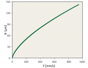
Using this approach, the data generat.edshowsthe contamination levelincrease on a silicon wafer after exposureand removal fom a wet process bath.Figure 2 shows the thickness of the film(h) left on a wafer after removal from a25'C water bath as a function of the with.drawal velocity (V).As Vincreases, so does the film thickness. Film thickness is quitesensitive at lower speeds, but becomesless dependent at hipher velocities. As thechemicals used in wet processing havesimilar surface tensions and densities.changing the liquid or its prperties viaadditives would have a modest effect onthe thickness of the liquid filmn.

Fi gure 2 - Thickness of the Film (h) left an a whfer After Removl From a 2sc WaterBath as a
Function of the WithdnwalVelocily (V).
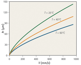
Because the viscosity of liguids isquite sensitive to change in temperature,increasing the temperature of the bathcan have a dramatic inflence on the filmthickness. Figure 3 shows the thickness ofa water film that remains after dipping a wa fer in a water bath at various tempera-tures (1).As the temperature rises, filmthickness decre ases with falling viscosity.For example, atV=100 mm's, h decreas.es from more than 30 m to less than 20um as Tincreases from 25° to 60C.

Figure 3 - Thickn ess of the Film (h Left on a Wafer After Removal From a Water Bath at Warious Temperatures (T).
Conclusion
It has been shown that impuritiesfound in a photovoltaic cell can reduce thecell's efficiency, lon contamination, forexample, will reduce the minority-carrierlifetime resulting in lower cell effciency.Consequently, it is functionally and financially iimportant to protect the siliconwafer from contamination during themanufacturing process. The data shownin this paper demonstrates the increase incontamination on a silicon wafer due tothe impurities found in the wet processes.This will allow photovoltaic manufactur-ers to evaluate their own wet processbaths and understand the impact theyhave on their wafer purity levels.
上一篇: 微流控芯片制造材料