Abstract—In recent days, 2.5D package designs have gained popularity with an increasing number of heterogeneous chiplets integrated into advanced system-in-packages. RDL wires become longer and denser, presenting a growing impact on system performance, reliability, and integrity. At present, there exists no standard CAD flow that can design, analyze, and optimize a complete heterogeneous 2.5D system. The traditional die-by-die design approach processes each component independently during extraction and optimization and cannot be applied to heterogeneous systems without fundamental changes in standard CAD tools. Not only the chiplet-package extraction is inaccurate between the die-package interface ignoring all RDL capacitive and inductive impacts, but traditional CAD tools are also unable to perform cross-boundary design optimization.
We present a complete chiplet-package co-optimization flow for both homogeneous and heterogeneous 2.5D designs. It encompasses 2.5Daware partitioning, chiplet-package co-planning, holistic and in-context extraction, package inductance consideration, and iterative optimization, along with design analysis and verification of the entire 2.5D system. In our previous work targeting heterogeneous systems, we achieved an extraction error ranging between -2.10% and 24.0%. The in-context design flow proposed in this work achieves less than 1% extraction error on ground and coupling capacitance. This extraction result can be used to perform timing analysis with 99.8% accuracy and to generate timing context with 99.4% accuracy for iterative optimization.
I. INTRODUCTION
The demand for increased functionality and performance in modern chips is ever-growing. In recent days, 2.5D integration is providing many design solutions within a compact package. Apart from reduced package size, 2.5D packages have lower power, higher bandwidth, higher yield, and better thermal dissipation. It reduces the turnaround time through plug-and-play design techniques. 2.5D integration has applications in IP-protection and hardware security. Heterogeneous integration also becomes one of the most attractive technologies, where chiplets from different technologies can be used in the same system.
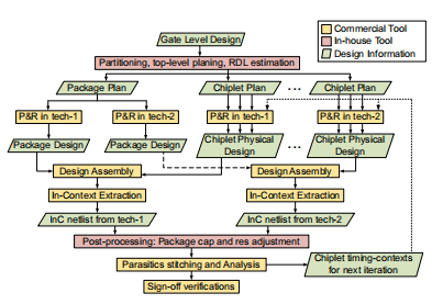
In this paper, we present our chiplet-package co-optimization flow for heterogeneous 2.5D systems. Our flow incorporates the features essential to perform accurate design, extraction, analysis, and optimization of the entire 2.5D system. In a holistic flow, a 2.5D system is analyzed as a complete system, chiplets and the package together. Fig. 1 illustrates our proposed flow for heterogeneous 2.5D systems. We employ an accurate in-context extraction strategy and perform adjustments using our in-house tools to create a holistic view of the system parasitics. We use these in-context parasitics to perform cross-boundary analysis and generate post-physical design timing contexts of all chiplets. Using these timing contexts, we perform iterative cross-boundary optimizations to ensure the best system-level performance. An in-context extraction strategy was first presented in [1] that can handle heterogeneous 2.5D systems. However, the extraction result was not accurate enough to ensure reliable analysis and timing context accuracy. In this work, our new in-context extraction method can achieve holistic-like accuracy and generate highly reliable analysis results and timing contexts for iterative optimizations. We claim the following new contributions: (1) A revised extraction strategy to perform in-context extraction of heterogeneous 2.5D systems; (2) A new post-processing method to improve the accuracy of extraction and analysis results; (3) A comparative study to validate the effectiveness of our methodology.

Fig. 1. Proposed in-context co-optimization flow for heterogeneous 2.5D systems
II. CHIPLET-PACKAGE CO-DESIGN FLOW
Our in-context flow for heterogeneous 2.5D systems is demonstrated in Fig. 1. Though the figure illustrates the flow for two heterogeneous technologies, the same methodology can be applied to a 2.5D system involving more than two technologies.
III. EXPERIMENTAL STUDY
In our experimental setup, we use an ARM Cortex-M0-based microcontroller system with two chiplets and 16KB memory, as presented in our previous work. The Core-Chiplet contains all the logic cells and 8KB memory, while the Mem-Chiplet contains the rest 8KB memory. We use a modified version of the Nangate 45nm PDK to implement the chiplets and the package, with the same settings as in Table 1 of . The lower seven metal layers are used with original settings to implement the chiplets. The top three layers are modified to mimic the attributes of high-density 2.5D package RDLs. We use standard cells from the Nangate 45nm cell library. Memory macros are compiled using OpenRAM memory compiler.

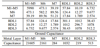
TABLE I COUPLING AND GROUND CAPACITANCES (IN FF) BETWEEN ROUTING LAYERS IN HOLISTIC EXTRACTION
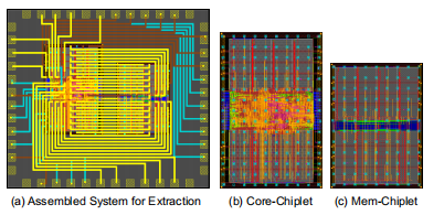
In the first iteration of the chiplet physical design, the chiplets are implemented using top-level constraints and estimated package wireload. Fig. 2(b)–(c) shows these chiplets finished designs. In the holistic design, we assemble both chiplets with the package, as shown in Fig. 2(a), and perform holistic extraction. We use this holistic extraction method to perform iterative optimization of the chiplets. From here on, we refer to this design as “Homogen-Holi” design. In the in-context design, only one chiplet is assembled at a time, and in-context extraction is performed on the assembled design. These in-context parasitics are adjusted using the methodology discussed in Section II. These in-context parasitics are used in the iterative optimization of the system. From here on, we refer to this design as “Homogen-InC” design.

Fig. 2. Chiplets and assembled package layouts of the homogeneous 2.5D system
IV. HETEROGENEOUS DESIGN CASE-STUDY
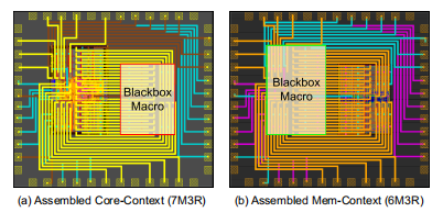
In this section, we present a design case-study of a heterogeneous system using 45nm technology. This is the same two-chiplet microcontroller system. However, in this design, the Mem-Chiplet is implemented using six metal layers and standard cells from the gscl45 cell library, which is bundled with the FreePDK45. CoreChiplet is implemented the same as before. Though fundamentally, both chiplets are using the same device node, from the tool flow perspective, it is still a heterogeneous system. Since there are two chiplet routing stacks involved in this implementation, two unified technology stacks are generated for package design and assembly: one with seven chiplet routing layers and three RDLs (7M3R), and the other with six chiplet routing layers and three RDLs (6M3R). The routing layer parameters are the same as in Table 1 of.

Fig. 3. Layouts of the assembled heterogeneous system for in-context extraction
VI. CONCLUSIONS
In this paper, we present our holistic and in-context design, extraction, analysis, and optimization flow for heterogeneous 2.5D systems. Through a comparative study between two implementations of a homogeneous system, we show that our in-context extraction methodology can achieve less than 1% error w.r.t holistic extraction method, which is a significant improvement from up to 24.0% error in our previous work [1]. This extraction method can achieve almost 100% accuracy in timing analysis and context generation. With a 45nm heterogeneous system combining two different PDKs, we show that our flow can optimize heterogeneous 2.5D systems and achieve holistic-like performance. Lastly, we discuss current limitations and further improvements of the flow, which will be explored in our future work.
上一篇: 湿法加工过程中污染物在硅介质上的沉积
下一篇: 半导体金属氧化物传感器路线图:回顾