Abstract: Identifying disease biomarkers and detecting hazardous, explosive, flammable, and polluting gases and chemicals with extremely sensitive and selective sensor devices remains a challenging and time-consuming research challenge. Due to their exceptional characteristics, semiconducting metal oxides (SMOxs) have received a lot of attention in terms of the development of various types of sensors in recent years. The key performance indicators of SMOx-based sensors are their sensitivity, selectivity, recovery time, and steady response over time. SMOx-based sensors are discussed in this review based on their different properties. Surface properties of the functional material, such as its (nano)structure, morphology, and crystallinity, greatly influence sensor performance. A few examples of the complicated and poorly understood processes involved in SMOx sensing systems are adsorption and chemisorption, charge transfers, and oxygen migration. The future prospects of SMOx-based gas sensors, chemical sensors, and biological sensors are also discussed.
1. Introduction
In sensing applications, metal oxides (MOxs (metal oxides), mainly II–VI semiconductors) are mostly used due to their inexpensiveness, ease of manufacture, quick response time, wide detection range, and resistance to harsh conditions. For sensors to be effective, (i) there must be a charge transfer between the analytes and sensing materials and (ii) the measurement must have an analyte concentration dependence . In addition, there is a need for efficient and effective methods for detecting volatile, chemical, and biological compounds and molecules. Analytical chemistry methods, such as spectrophotometry, fluorometry, gas chromatography (GC), and high-performance liquid chromatography (HPLC), were previously used to detect these molecules accurately. Furthermore, these methods were heavy, expensive, had low throughput, time-consuming pretreatment steps, required highly skilled operators and significant power consumption, and did not provide real-time information for risk reduction or decision-making . As a result of these limitations, most present sensing methods rely on SMOx-based materials for sensing applications, such as 1D and 2D field effect transistors (FET) and the Internet of things (IoT).
2. Fundamentals of Semiconductor Metal Oxides
The easy charge transfer properties of metal oxides (MOxs) make them unique among semiconducting materials. This effect is due to the large electronegativity difference, and thus, the high degree of ionic bonding, between the metal and oxygen that the MOx has. MOx has a conduction band minimum (CBM) and valence band maximum (VBM) of metal (M) ns and oxygen (O) 2p orbitals, respectively. Metals (Ms) and oxygen (O) have highly dispersed or localized orbitals (ns and 2p). Furthermore, metal oxides have a much higher dispersive valence band maximum (VBM) than n-type semiconductors. As an example, In2O3, ZnO, SnO2, and their hybrid composites function as n-type MOx, while NiO and Cu2O are p-type MOx. The first-known p-type transparent conductive oxide (TCO) was nickel oxide (NiO).
3. Properties of Semiconductor-Metal-Oxide-Based Sensors
Regarding the greenhouse effect, MOx-based sensors are used for the rapid detection of harmful and toxic gases, where the low concentration (in ppm or ppb) of the target gas is converted into a measurable electrical, optical, or magnetic signal. In these sensors, metal oxide semiconductors and metal oxide–polymer composites are used to produce excellent sensitivity. As a result, semiconducting metal oxides (SMOxs) can be used to detect low gas concentrations with a high sensitivity and rapid response. A SMOx-based sensor is characterized by its low cost, rapid response and recovery time, high stability, simple electronic interface, and low maintenance, making it an ideal and promising material for detecting toxic gases . Materials made of SMOx are ionic solids, which are held together by strong ionic bonds between positive metallic and negative oxygen ions. Semiconductor metal oxides (SMOxs) have filled electronic shells, making them more thermally and chemically stable than free metal oxides. Incomplete electronic shells d endow optical properties, such as high dielectric constants. Depending on the design, a SMOx can be flexible; porous; and can be in a zero-dimensional shape (0D), a 1D shape, a 2D shape, or a 3D shape. As the temperature increases, SMOx materials’ conductivity (and hence resistance) changes. Moreover, optical, electrical, and magnetic fields affect the conductivity of SMOx.
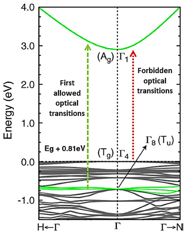
In addition, the sensing property of n-type semiconductors and p-type semiconductors depends on the energy band structure of semiconductor metal oxides (SMOxs). When the SMOx thickness reaches a level comparable to the depletion layer width, the energy band is no longer constrained to the surface but is affected by a significant number of grains, which, in turn, affects the electronic structure and electron–hole charge carriers . In general, an electron’s conduction energy band becomes vacant when the minimum band gap energy (Eg) of the SMOx is reached (Figure 1). As a result, the valence band is left with holes. Electrons (e−) and holes (h+ ) are easily mobilized in the presence of an external electric field, while at low energy, electron–hole pairs (e− + h+ ) are electrostatically bound . Since In2O3 has a small effective mass of electrons, its band structure shows a highly dispersive CBM. Its optical bandgap is 3.7 eV . The presence of impurities induces intra-band electron transitions, such as electrons moving from defect states to ground states. By adjusting the size, shape, and composition of impurities, intraband gaps can be modulated. A SMOx sensor with a large Eg can work at high temperatures, which indicates that SMOx sensors are thermally stable. When the operating temperature exceeds 300 ◦C, gas sensors should have a band gap greater than 2.5 eV. SMOx-based gas sensors have a weakly dependent chemical activity on ambient humidity (Figure 1). In some core–shell semiconductors, for instance, the conduction and valence bands of the core and shell are staggered, and electrons and holes are separated. It was found that the conduction band energy was the lowest in the shell and highest in the core. The energy band offsets in semiconductor materials segregate electrons from the shell and holes from the core, allowing carrier recombination across the interface at a lower energy than any of their constituent band gaps . Electronsaturation velocities are high, heterojunctions are readily available, gaps are broad, and breakdown fields are large, allowing for fast and very sensitive gas detection systems to operate. The size and shape of semiconductor materials can be controlled by applying strain due to quantum confinement phenomena. It is possible to adjust the bandgap range of semiconducting nanostructures due to their high elastic limit. The band structure governs the adsorption of light, charge separation, and recombination of charge, which determines the use of a SMOx in photoelectric conversion.

Figure 1. Band structure of In2O3 near the Brillouin zone. Here, a weak optical absorption is observed at 2.7 eV and a strong optical transition occurs between lower − lying valence bands
Carrier Transportation and Electronic Structure of SMOx
Conductivity in semiconductor metal oxides is affected by the production of free carriers, e.g., electrons in n-type semiconductors and holes in p-type semiconductors . A stable concentration of conductive electrons and holes is maintained at thermal equilibrium . Metal oxide’s electronic structure, temperature, applied electronic field, doping, and lack of structural order in the material can influence carrier transport mechanisms, such as drift, diffusion, and recombination. The movement of carriers from a high concentration to a low concentration is called diffusion. Also, the carrier recombination rate affects the carrier lifetime and gas-sensing properties.
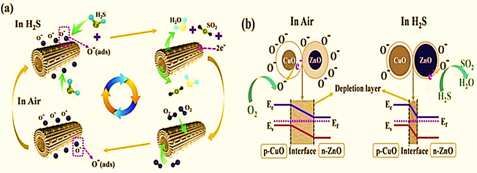
Generally, p-n junctions form between semiconductors with different electronic structures. A hole diffuses from a p-type semiconductor to a n-type semiconductorleaving negatively charged ions on the p-type semiconductor. The n-type semiconductorhowever, loses free electrons, leaving positively charged ions. p-n junctions possess unidi.rectional conductivity since the ions cannot diffuse and form a zone of space charge at theinterface. A p-n junction affects the electronic, optical, and magnetic properties of SMOxmaterials . It is possible to control the properties of SMOx to design it for a widerange of applications, such as gas sensing, catalysis, and energy storage. C. Han and coworkers presented hollow nanofibers based on p-CuO/n-ZnO for gas sensing [130]. Usingatomic layer deposition (ALD), electrospun heterostructures were fabricated to investigatethe effect of the composition on gas sensing. As the concentration is increased, the responserate slowly decreases, with Rzn/cu = 15.6. Compared with pure ZnO and pure CuO, theseheterostructures exhibit 6 and 45 times higher responses to H,S gas, respectively (Figure 2).

Figure 2. Schematic illustration of (a) H,S gas detection via hollow nanofibers and (b) the formation of the depletion layer at the p-n interface
4.Conclusions
A SMOx-based sensor translates a response into an electrical signal by using a receptortransducer device. A wide range of applications, such as the detection of diseases and illnesses, environmental monitoring, water and food quality monitoring, and drug delivery, prompted scientists and researchers to develop more sensitive and selective sensors. SMOx-based sensors need to capture recognition signals efficiently and convert them into electrochemical, electrical, optical, gravimetric, or acoustic signals (transduction process). Increasing transducer performance is another challenge, as it allows for increased sensitivity, faster response times, reproducibility, and lowering detection limits, even to detect single molecules and miniaturization of the sensing devices. Combining sensing technology with nano-SMOx-based devices, like zero- to three-dimensional FETs and IoT, with high surface-to-volume ratios, good conductivities, shock-bearing properties, and colour tuning can overcome these challenges. In this review, we provide an overview of the development of SMOx-based sensors.