Abstract: Wide Band Gap (WBG) semiconductors have the potential to provide significant improvements in energy efficiency over conventional silicon (Si) semiconductors. While the potential for energy efficiency gains is widely researched, the relation to the energy and resource use during manufacturing processes remains insufficiently studied. In order to appraise the performance of the technology thoroughly, issues such as raw material scarcity, toxicity and environmental impacts need to be investigated in detail. However, sparse Life Cycle Assessment (LCA) data are available for the two currently most widespread WBG semiconductor materials, gallium nitride (GaN or GaN/Si) and silicon carbide (SiC). This paper, for the first time, presents a cradle-to-gate life cycle assessment for a GaN/Si power device. To allow for a full range of indicators, life cycle assessment method EF 3.1 was used to analyze the results. The results identify environmental hotspots associated with different materials and processes: electricity consumption for the processes and clean room facilities, direct emissions of greenhouse gases, gold (when used), and volatile organic chemicals. Finally, we compare this result with publicly available data for Si, GaN and SiC power devices.
1. Introduction
Rapidly transitioning the world away from the use of fossil fuels to cleaner renewable forms of energy is essential if the world is to meet climate targets. Part of greenhouse gas emissions reduction could be achieved with the use of renewable energy and a high rate of electrification instead of fossil fuels. The broader application of wide bandgap (WBG) semiconductors for power electronics carries the promise of large energy savings in a range of different applications, including inverters for photovoltaic systems, power supplies for consumer electronics, uninterrupted power supplies for data centers and drive-trains and charging infrastructure for the electric automotive sector. WBG semiconductors are characterized by bandgap energies three or more times that of Si, enabling them to withstand much higher voltages. Consequently, WBG devices can be made much smaller, allowing faster switching with less resistance. Because of the reduced resistance, less energy is wasted as heat compared with Si devices, making WBG more energy efficient. While these energy efficiency improvements from using WBG components compared with Si-components are widely researched and promoted by manufacturers, the environmental impacts along the entire life cycle (beyond the use phase) are far less understood. Moreover, to the best knowledge of the authors, there is currently no Life Cycle Assessment (LCA) data available specifically focusing on WBG semiconductors, and (publicly) available LCA information of sufficient level of detail and quality is limited or outdated. This is due to process complexity involving numerous process steps and specialty chemicals in energyintensive clean rooms, and rapidly evolving technology in a competitive and secretive industry. In addition, most of the current research available in the field of semiconductors focuses rather on Si-based semiconductors for information technology or solar cells and does not take into account specificities of power semiconductors such as wafer thickness, specific processing, number of mask levels, etc. In this paper, we evaluate the environmental impacts at the fabrication of a GaN/Si transistor, of specifications 650 V and 30 A , on a CMOS-compatible process flow on 200 mm Si substrate, with LCA methodology.
2. Methodology and Scope
Life cycle assessment (LCA) is a method that helps investigate the environmental impact of a product from raw material extraction to disposal or recycling. This is achieved by quantifying all materials and energy inputs as well as waste and pollutants outputs, enabling the comparison of the impacts of products manufactured and used for the same purpose. The present LCA study was performed according to the international standards, ISO 14040 and ISO 14044 , using SimaPro software with the ecoinvent v3.9 database. The EF 3.1 methodology was applied to analyze the results, as recommended by the European Commission.
Following this analysis, a “cradle-to-gate” approach, which only takes into account impacts occurring from raw material extraction to the production gate, was preferred, as the use phase depends on the chosen system and its technical performance, Figure 1.

Figure 1. Drawing showing the system boundary detailing the stages included into this cradle-to-gate analysis. It only consists of the manufacturing stage of device production, starting with raw material extraction, through processes for the production of a wafer, followed by dicing and packaging of the inaging of the individual devices (“dies”) into trans.
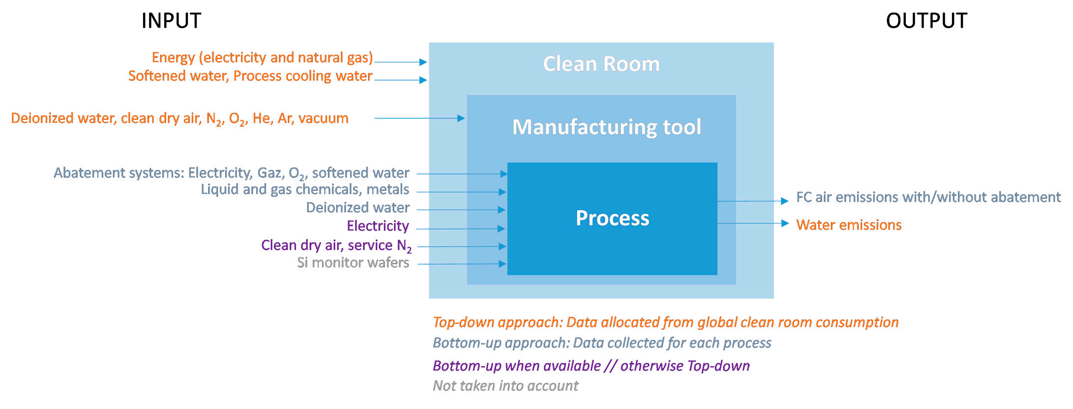
Inventory data have been collected, where available, in the cleanroom. Missing datawere modeled, based on data collected from patents, publications or industrial data sheetsAn hybrid approach was chosen, imaged in Figure 2 and described hereafter.

Figure 2. Shows the hybrid top-down and bottom-up approach used for semiconductor device manufacturing LCI in this study
3. LCI, LCA Results
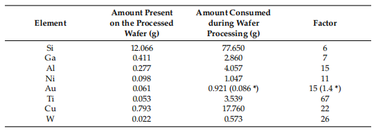
In this study, the GaN MOSc-HEMT processing requires 17 mask levels (10 for the front-end processing or FEOL, six for the back-end processing or BEOL, and one for wafer substrate thinning, which is specific to the chosen packaging) and 118 processing steps. Power semiconductors like MOSFETs and diodes require far fewer mask levels compared with memories, processors or logic chips, e.g., SiC IGBTs require about 11 to 12 mask levels . FEOL requires 56 process steps; BEOL, 50 process steps; and Si wafer thinning, 12 process steps. For a 200 mm wafer, after processing and Si substrate thinning, the material amount present on the wafer is between 6 and 67 times lower than what was necessary for the processing, as shown in Table 2. The amount of material that must be extracted to produce a certain amount of metal commodity is even greater, with a rock-to-metal ratio from 3 for Si to 3 × 10⁶ for Au.

Table 2. Shows the amount of various elements present on the wafer and the amount that is consumed (elemental, as calculated from gas or liquid precursor quantity) during wafer processing. * Gold is recovered from the deposition chamber.
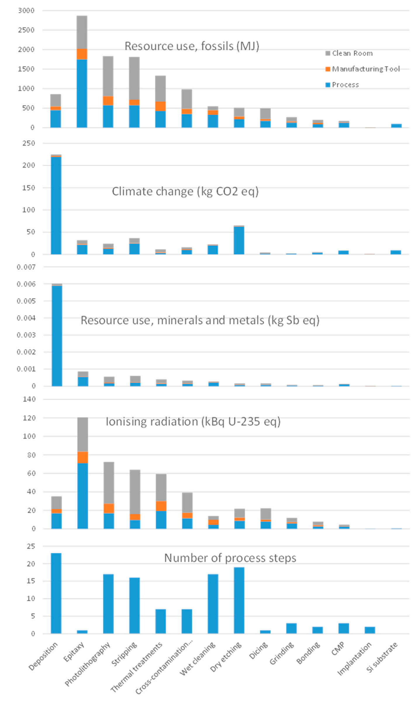
After normalization and ponderation, the following impact categories are selected: resource use, fossils; climate change; resource use, minerals and metals; and ionizing radiation, accounting for 81% of the unique score (total of 55.7 mPt). The main environmental impacts for the production of a wafer are presented in Figure 3.

Figure 3. Main environmental impacts and number of process steps for the processing of a 200 mm GaN/Si MOSc-HEMT wafer presented by process category and by contribution (process, manufacturing tool and clean room.
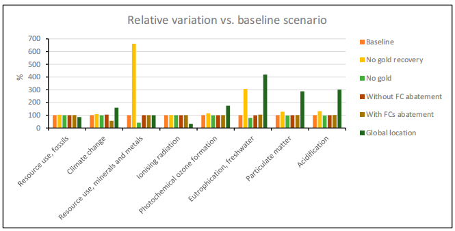
The impacts of the choice to abate fluorinated compounds are evaluated. FC emissions into air are calculated using destruction removal efficiency (DRE) abatement rates, and additional consumptions (water, natural gas, electricity, O2) of the abatement systems are added for the seven PECVD, one CVD and two dry-etching steps using FCs in the process recipe, not already abated. After normalization and ponderation, the following impact categories are selected: resource use, fossils; resource use, minerals and metals; climate change; ionizing radiation; and photochemical ozone formation, accounting for 83% of the unique score (total of 50.6 mPt, (see Table 4). Since the impacts associated with climate change are reduced, the impacts on photochemical ozone formation become apparent on single score results, even if it does not increase from the baseline scenario. FC emissions into air are also calculated for a scenario without any abatement system for the three dry-etching process steps using FCs in the process recipe, already abated in the baseline scenario. In this case, the main indicators are resource use, fossils; climate change; resource use, minerals and metals; and ionizing radiation, accounting for 81% of the unique score (total of 56.2 mPt). Since fluorinated compounds have a high impact on climate change, taking into consideration the absence or presence of abatement can lead to an increase of 5% or a decrease of 43% of the impacts (see Figure 4). Therefore, it is important to properly assess the amount of fluorinated compounds used in the processes, the formation of by-products and the destruction removal efficiencies.

Figure 4. Relative variation of main im pact categories according to different 200 mm MOSc-HEMTwafer prduction scenarios with variation from the baseline.
4. Discussion
It has been reported that Si chip manufacturing (IGBT and diodes, total chip area 9 cm2 ) contributes significantly to the environmental impacts of power module manufacturing, which is itself an environmental hotspot in a 150 kW traction inverter. The main reported environmental impacts are on climate change, ozone depletion, ionizing radiation and fossil material consumption. Since WBG power semiconductors are able to fulfill the same function with a smaller die, one can expect a reduction of the environmental impacts compared with Si. However, for SiC semiconductors, additional processing steps are needed to obtain the SiC powder and to grow SiC wafers. For GaN/Si semiconductors, epitaxy is necessary in order to grow the III-N layers.
It is clear that publicly available LCA information of sufficient level of detail and quality is limited, especially when communicated by manufacturers, as limited information on electrical specifications or die size are available. Musil et al. assessed the climate change environmental impacts for the production of Si and SiC dies by extrapolation of energy requirements for Si wafers and Si wafer processing from the ecoinvent database and adding energy requirements for SiC wafer production . Li et al. assessed the climate change environmental impacts for the production of Si, taking into account the mass of the chip (assimilated to silicon) and electricity requirements for front-end processing. The Navitas study reports the climate change impacts of WBG being up to four times lower compared with a Si power semiconductor (Si FET) with today’s production, and could be 10 times lower in the future as wafers of larger diameters are fabricated. At this stage, it is not possible to conclude on potential improved or reduced environmental impacts for the manufacturing of WBG compared to Si power devices, even if it seems that reducing the die size has a great effect on the reduction of the impacts.
5. Conclusions
For the first time, a detailed cradle-to-gate life cycle assessment has been carried out for the manufacturing of a GaN/Si power device (MOSc-HEMT technology on 200 mm Si wafers), based on in-house CEA-LETI R&D microelectronics clean rooms.
Semiconductor wafer processing is material- and energy-intensive, with between 6 and 67 times more metals needed for the processing than present on the wafer, and consumptions of 194 g of chemicals (gases and liquids), 33 L of water and 2 kWh of electricity per cm2 of processed wafer. High energy consumption of the processes and of the clean room facilities leads to environmental impacts on resource use, fossils; ionizing radiation; and climate change. Due to high electricity consumptions, these impacts are dependent on the electricity mix at the manufacturing location and may vary. Direct emissions of greenhouses gases such as fluorinated compounds during deposition or dry-etching processes have a high impact on climate change, which can be reduced with appropriate gas-abatement systems. The use of volatile solvents leads to impacts on photochemical ozone formation. The eventual presence of gold metallization or wire bonding in the wafer processing or in the packaging leads to high impacts on resource use, minerals and metals. Gold should be, at a minimum, recovered from the processing, and substitution materials should be preferred.