Abstract—Traditionally, different components of a system are integrated through Printed Circuit Boards (PCB). The long traces on PCB have severe power loss and limit the bandwidth of the interconnects between the components. Advanced packaging offers high-bandwidth, low power, and high-performance inter-die communications with compact sizes and dense pin arrays. 2.5D integration further provides better thermal dissipation, lower cost, and higher yield compared to 3D stacking. Novel CAD tool flows dedicated to 2.5D chiplet designs are essential to enable flexible and efficient 2.5D system designs. In this paper, we present our design, optimization, and analysis methodologies and a design case study implementing an ARM Cortex-M0 microcontroller system using a holistic 2.5D tool flow. We use TSMC 65nm as our chiplet implementation technology with a modified metal stack referring to 2.5D Fan-Out WaferLevel Packaging (FOWLP) solutions. We also discuss design techniques for chiplet reuse and the Drop-in design approach to develop low-power, low-cost, and high-performance flavors of a 2.5D system. We compare the 2.5D system with its 2D counterpart to validate the holistic design flow.
I. INTRODUCTION
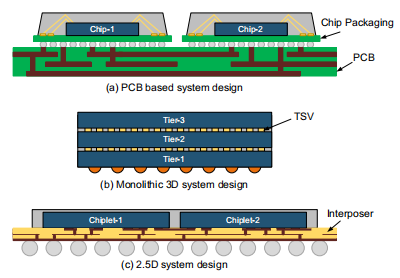
To support the ever-growing demand for increased functionality and performance, the sizes of modern chips such as GPU, FPGA, AI accelerators are reaching the reticle limit. Increased chip-size comes with high design complexity, longer wire-lengths, higher power consumption, and lower yield. As a result, the industry has developed the System-in-Package (SiP) design approach, where a complicated system is divided into smaller chiplets and then integrated as a whole system on the package. This modular design offers increased flexibility, reduced complexity, short chip wire-lengths, and heterogeneous integration. Traditionally, a Printed Circuit Board (PCB) is used as the system integration platform. Illustrated in Fig. 1(a), PCB design is simple, fast, and cheap. However, the interconnections through the PCB have long wirelength, high inductance and capacitance, limited bandwidth, and suffer from severe power and signal loss. As a result, the industry has developed 2.5D and 3D packaging for energy-efficient inter-chip communications. Fig. 1(b) and (c) illustrate a TSV-based 3D IC and a silicon-interposer-based 2.5D system, respectively. Previous studies have demonstrated orders of magnitude improvement on interconnect bandwidth and power efficiency in 2.5D and 3D systems compared to PCB-based systems. Along with these benefits, 2.5D and 3D system designs offer a compact package size, which makes them attractive candidates for portable devices. However, though 3D ICs have smaller form factors and higher bandwidth compared to 2.5D systems, it suffers from poor thermal dissipation and lower yield. The Wafer Level Packaging (WLP) process using Know-Good-Dies improves performance, power consumption, and cost of production of 2.5D systems. Moreover,a 2.5D system provides heterogeneous integration capability, where technology-specific optimization techniques can be applied to individual chiplet to further reduce the overall area and power consumption of the system. As a result, the 2.5D design approach is the most attractive candidate, especially for cost-sensitive low-power mobile systems.

Fig. 1. System Design technologies: (a) PCB based system (b) TSV based monolithic 3D system (c) High density 2.5D integration scheme
In recent years, both industry and academia are investing great efforts in the development of 2.5D integration technology. Various integration schemes like Flip-Chip (FC), Package-on-Package (PoP), Ball-Grid-Array (BGA) have been explored using various substrate materials, including glass, ceramic, organic, and silicon. At this moment, there exist a few advanced high-density options like eWLB, SWIFT, and InFO [3]. To drive the interconnects through interposer layers novel high-speed and low power I/O circuits are developed with standard interface protocols. Novel system design approaches like plug-and-play and Drop-in methods are also investigated for agile ASIC design. Dedicated algorithms and strategies to perform floorplanning, package routing, I/O redistribution of 2.5D systems are proposed. A recent published work presented a holistic design methodology that can design, optimize, and analyze a complete 2.5D system using standard ASIC design tools. In this paper, we demonstrate the application of the holistic flow on a practical chip design technology (TSMC65nm) and present the analysis results. We also present a shared-block tape-out technique to design a chip that can be used for a comparative study between the 2.5D system designed in the holistic flow and a reference 2D system. This chip is fabricated on silicon to validate the flow.
II. DESIGN SETTINGS AND CAD FLOW
A. System Architecture
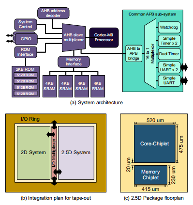
The micro-controller system has an ARM Cortex-M0 processor core, 16KB of memory, bootloader ROM, and some common peripheral devices. The entire system organization is shown in Fig. 2(a). The AHB bus is connecting the processor core to an AHB address decoder, a system controller module, an APB sub-system, two GPIO modules, the ROM interface, and the memory interface. The APB sub-system is connected to the AHB bus through a multiplexer and an AHB-to-APB bridge. The UARTs of the APB sub-system share pins with the GPIO ports to reduce the system pin count. The bootloader ROM is 2KB in total and is divided into four 512B banks. The data memory system consists of four 4KB memory blocks.

Fig. 2. (a) Architecture of the ARM Cortex-M0 micro-controller system (b) Integration floorplan for shared-block system design (c) Package floorplan generated by RDL planner tool
B. Technology Settings for Tape-Out
To reduce the I/O pad overhead and satisfy the minimum chip area requirement, we perform a shared-block tape-out where the separately designed 2D and 2.5D systems are taped-out in a single die with shared I/O pads. Fig. 2(b) illustrates our shared-block tapeout plan. The two microcontrollers have their own independent I/O sub-systems. We design an I/O multiplexing module that receives the I/O signals from both systems and bridge any one of them with the external world. The two systems also share the Power Distribution Network (PDN) of the die. This shared-die shared-I/O design technique can be used to design a chip containing multiple small sub-designs for comparative study among them. This will reduce the tape-out cost and also make the measurement results independent of process variations.
We implement the aforementioned system using the standard cells and memory compilers from ARM for the TSMC 65nm technology. For the physical design, we use M1 to M6 to perform routing of the 2D chip and the internal routing of the 2.5D chiplets. A holistic design flow requires a unified PDK that can handle both chiplet and package in the same design environment. As depicted in Fig. 3, M7 of the original technology corresponds to the contact pads of the chiplets. M8 is modified to mimic the first package routing layer (RDL1) that connects to the chiplet contact pads. M9 layer corresponds to the second package routing layer (RDL2). The solder pads will be placed on another layer, which is next to RDL2 and corresponds to the AP layer of the original technology.

Fig. 3. Our modified 65nm package redistribution layer stack
V. ANALYSIS RESULTS
A. Holistic Extraction Results
Table III presents the holistic extraction results obtained after assembling the chiplets and package designs at the top-level. For readability, we merged the coupling capacitances among layers M1- M3 in the table. As seen from the table, the holistic extraction method effectively captures the interactions between the chiplet and package wires. Using traditional extraction flows, one can get the results in the second quadrant (among intra-chiplet layers) and fourth quadrant (among package routing layer). Even though, our design is a small system there exists sufficient coupling between RDL1 and top chiplet layers like M4-M6. In a large system with a lot of package wires and denser chiplet routing on the top routing layers, these couplings will be severe and if ignored may cause signal integrity issues leading to total system failure.
B. Timing and Power Analysis Results
Table IV presents the timing and power analysis results. The standard cell count of the Core-Chiplet and the 2D chip are comparable. As mentioned in Section III-D, the optimization steps of chiplet design insert some buffers/inverters which is why the MemChiplet has those 27 standard cells apart from the SRAM macros. The total wire-length at the chiplet level is shorter in the 2.5D system compared to the 2D chip. This result is consistent with a previous study which reveals the reduction of total chip wire-length in 2.5D design. The overall performance of the 2.5D system is worse than the 2D system because of the package wire overhead. The maximum system frequency we could achieve is 125MHz for the 2D system and 100MHz for the 2.5D system; the performance gap being 20% w.r.t the 2D system. This result is also consistent with the previous study , where the 2D system achieved an operating frequency of 333MHz while the 2.5D system could only achieve 245MHz, a 26% performance gap w.r.t the 2D system. The power numbers in the table correspond to the maximum system frequency. The lower power of the 2.5D chiplets is because of the reduced system frequency.
C. Chip Testing and Validation
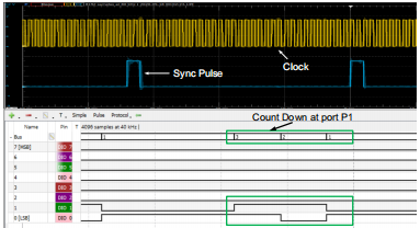
The fabricated chip is tested and validated using test vectors generated by a logic analyzer. Fig. 8 shows one of the testing waveforms. In this test, the micro-controller reads a top value from a GPIO port and performs count-down on another port. After each countdown is finished, it sends a synchronization pulse to the logic analyzer. The fig. 8 shows the clock signal, synchronization pulse, and the count-down on a digital bus connected to the GPIO port.

Fig. 8. Chip testing waveforms from logic analyzer
VI. CONCLUSION
In this paper, we present the entire design methodology of a 2.5D system in a commercial chip design technology, starting with its RTL netlist to the sign-off verification of the final GDS. We follow a holistic design, optimization, and analysis flow to implement an ARM Cortex-M0 processor-based micro-controller system in TSMC 65nm PDK to be integrated using TSMC InFO technology. The design techniques presented for shared-block tape-out and application of Drop-in design approach can be used for low-cost, low-power, and high performance applications. This design case study validates the effectiveness of the holistic design and analysis flow for 2.5D system designs in real-world technologies. From our extraction results, we can conclude that the holistic extraction process effectively captures the interactions between different components of a 2.5D system across chiplet and package layers. Our timing and power analysis results reveal that the holistic analysis approach takes into account the impacts of package overhead on system performance, which is essential for reliable system design.