Desired electrode patterning on two-dimensional (2D) materials is a foremost step for realizing the full potentials of 2D materials in electronic devices. Here, we introduce an approach for damagefree, on-demand manufacturing of 2D material devices using light-emitting diode (LED) lithography. The advantage of this method lies in mild photolithography by simply combining an ordinary optical microscope with a commercially available LED projector; the low-energy red component is utilized for optical characterization and alignment of devices, whereas the high-energy blue component is utilized for photoresist exposure and development of personal computer designed electrode patterns. This method ofers maskless, damage-free photolithography, which is particularly suitable for 2D materials that are sensitive to conventional lithography. We applied this LED lithography to device fabrication of selected nanosheets (MoS2, graphene oxides and RuO2), and achieved damage-free lithography of various patterned electrodes with feature sizes as small as 1–2 μm. The LED lithography ofers a useful approach for cost-efective mild lithography without any costly instruments, high vacuum, or complex operation.
Recent advances in 2D materials provide great promise for next-generation electronics owing to their unique properties at atomic thickness . Desired electrode patterning on 2D materials is an essential and foremost step for realizing new electronic devices. Photolithography and electron beam (EB) lithography are well-established techniques for site-specifc and on-demand nanofabrication with high-resolution patterning. However, these techniques have some drawbacks, such as high cost of instruments, high vacuum, complex operation, low throughput, and processing damage, which signifcantly limit their utility. For example, conventional photolithography (or UV lithography) normally requires the premanufacture of custom-made hard photomasks, which are very expensive, time consuming to produce and ofen limit the fexibility. Te EB lithography ofen causes inadvertent impurity doping and crystal damage; the atomically thin nature of 2D materials renders them prone to beam damage during the EB lithography and to degradation of their superior electrical properties. Without addressing these issues, the potential advantages of employing 2D materials may be greatly reduced. Te development of facile mild lithography that enables damage-free, on-demand manufacturing of 2D material devices without costly instruments or complex operation is urgently needed.
Results and discussion
Device fabrication based on LED lithography.
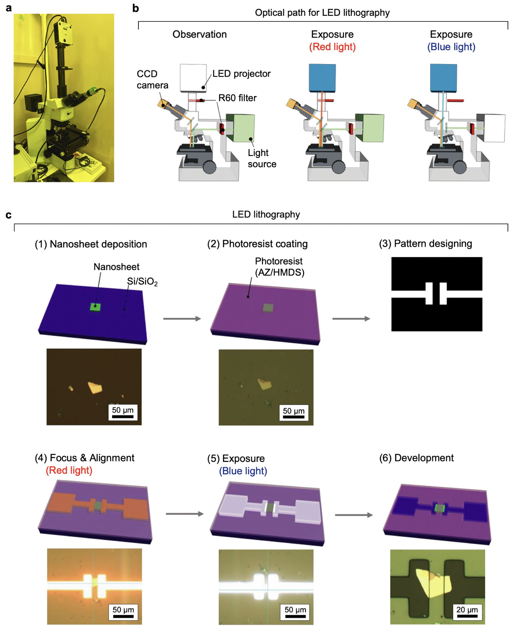
Figure 1a shows a photograph of the LED lithography system. Te LED lithography system is mainly composed of four parts: an optical microscope, an LED projector, a computer, and a charge-coupled device (CCD) camera, where the camera and projector parts are connected to ocular and adapter lenses, respectively. To protect the photoresist layer from unexpected exposure, two red sharp cut flters (R60,≤600 nm) were applied to the light sources of the optical microscope and the LED projector. Te details of the optical paths are illustrated in Fig. 1b. During observation, the light from the projector was cut of, and the optical microscope could provide observation of the nanosheet position for address-free pattern alignment of the nanosheets. During exposure, the light from the microscope was cut of so that the patterns at the designated location could be exposed by the LED projector.

Figure 1. LED lithography. (a) Photograph of the LED lithography. (b) Schematic illustration of the optical pass for the LED lithography. (c) A typical procedure for the LED lithography. Te upper part shows a schematic illustration for six steps, together with the corresponding photographs (lower).
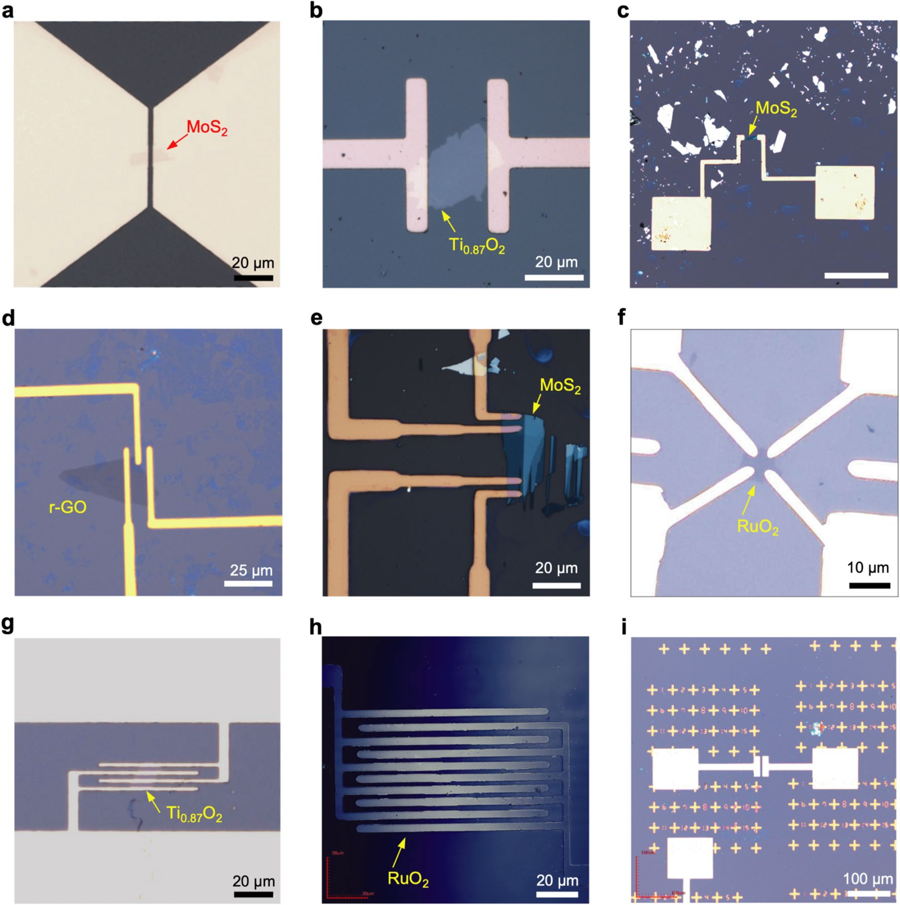
We applied the LED lithography to pattern the metal contacts of nanosheet devices (Fig. 1c). Te process for LED lithography includes six steps: (1) nanosheet deposition, (2) photoresist coating, (3) pattern design, (4) alignment using red light, (5) exposure to blue light and (6) development. Te process began by depositing 2D nanosheets on 90- or 290-nm SiO2/Si substrates via drop casting. Ten, hexamethyldisilazane (HMDS) was spincoated on the sample surface as a hydrophobic treatment to enhance the adhesion of the subsequent photoresist layer. We chose AZ1500 (4.4 cp, Merck group, USA) as a photoresist10 because of its blue-light sensitivity and good compatibility with the developer as it can be easily developed without residues. A 500-nm-thick photoresist layer was deposited by spin-coating it on the HMDS layer and baking the flm at 90 °C for 3 min. Afer flm preparation, the pattern of metal contacts designed by a PC was aligned by optical microscope, and the position and focusing of the pattern were checked under exposure to red light. Afer fne adjustment, the high-energy blue component was employed for the exposure of the photoresist layer. Finally, the exposed region of the photoresist layer was removed to form the mask for the patterned metal contacts, followed the development process with tetramethylammonium hydroxide (NMD-3) solution (2.38%). Afer the LED lithography, a metal layer (such as Au or Ti/Au) was deposited by electron beam evaporation on the developed flm. Te resultant flm was then immersed in acetone at 50 °C for 1 h to lif of the extra metal coating. Figure 2 shows several examples of 2D devices fabricated by the LED lithography. Trough PC-based mask design and appropriate alignment, we successfully fabricated several types of 2D devices, including two-terminal, multiterminal, and interdigitated devices, and designed patterns (Supplementary Fig. 1).

Figure 2. 2D nanosheet devices fabricated by the LED lithography. (a) Two-terminal device of 1L MoS2. (b) Two-terminal device of 1 L Ti0.87O2. (c) Two-terminal device of 1 L MoS2. (d) Tree-terminal device of 1 L r-GO. (e) Four-terminal device of 1 L MoS2. (f) van der Pauw device of 1 L RuO2. (g) Four-terminal device of 1 L Ti0.87O2. (h) Interdigitated device of 1L RuO2 flm. (i) Address patterns.
Characterization of patterned microstructures.
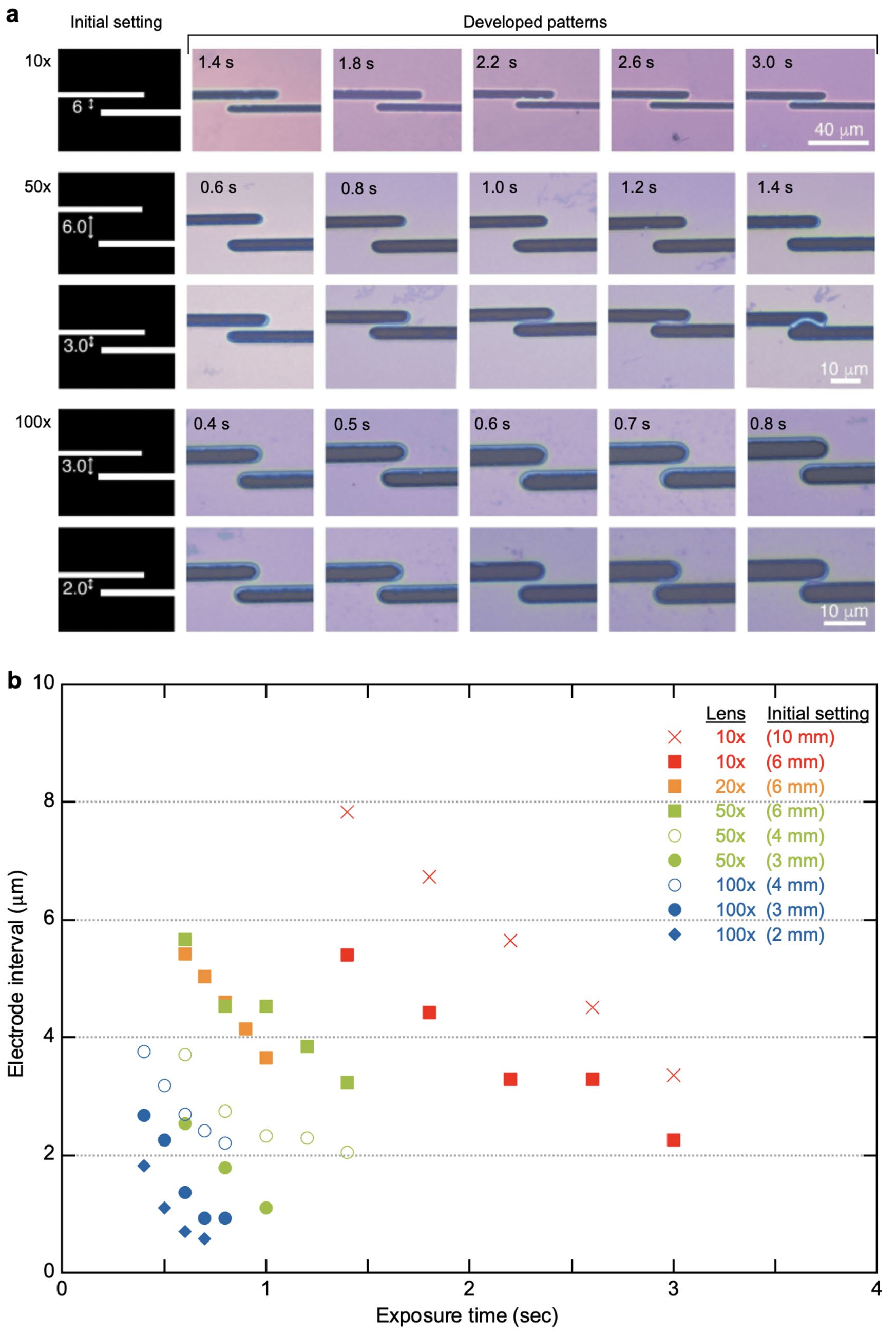
To demonstrate the patterning capability, we investigated the exposure conditions using four diferent objective lenses (with 10×, 20×, 50×and 100×magnifcations). Figure 3a highlights the dependence of the developed patterns on the exposure condition in comparison with the initially designed patterns (lef). Te patterning capability and device structures were characterized by the confocal laser microscopy. All data are shown in Supplementary Figs. 2–6. Clearly, the magnifcation of the lens strongly afects both the development rate and resolution. Since the power density of the exposure light is inversely proportional to the spot diameter, higher magnifcation lenses yield enhanced power densities, resulting in faster development. A short exposure time was needed for higher magnifcations. We also note that exposures with diferent magnifcations can produce electrodes with various feature sizes and gaps. Figure 3b illustrates the infuence of the exposure time on the electrode interval. For a pair of electrode patterns with a set distance, a prolonged exposure time would result in shrinkage of the electrode interval. For the lower magnifcations (10×and 20×), the minimum gap size reached 3 μm. Te use of higher magnifcations (50×and 100×) with a high numerical aperture (NA) (0.75) could improve the resolution, but also cause expansion of the developed area. For a prolonged exposure time, two electrode patterns merged into a gapless feature. For the 100×magnifcation, the fnest features were obtained during the short exposure time (0.4–0.6 s); the minimum electrode width and gap were 2 and 0.7 μm, respectively. To check the minimum gap, we also fabricated the gap electrodes with various settings (Supplementary Fig. 7). Te minimum gap attained with the 100×magnifcation reached~0.57 μm, which is suitable for device fabrication using small nanosheets with a lateral size of 1–2 μm.

Figure 3. Patterning capability. (a) Te dependence of the developed patterns on the exposure condition in comparison with the initially designed patterns (lef). Two electrodes fabricated by LED lithography with diferent objective lenses (×10, ×50and ×100) and various exposure time. (b) Te relationship between the electrode interval and the exposure time. We evaluated the electrode intervals fabricated by diferent objective lenses with various initial settings.
Conclusion
We have demonstrated a simple and rapid manufacturing of 2D material devices using the LED lithography. In the LED lithography, the PC-designed pattern can precisely be located and rapidly developed on the photoresist layers by the LED projector so that maskless photolithography can be achieved, free from the process damage ofen encountered in the conventional lithography. Tis method is particularly suitable for 2D materials with sensitivity to conventional EB lithography. We applied this LED lithography to device fabrication of selected nanosheets (MoS2, GO, r-GO and RuO2), and achieved damage-free lithography of various patterned electrodes with feature sizes as small as 1 μm. Our method enables the on-demand device fabrication of 2D nanosheets free from the processing damage, providing a detailed glimpse of the true properties of 2D nanosheets