Abstract: Since the avalanche phenomenon was first found in bulk materials, avalanche photodiodes (APDs) have been exclusively investigated. Among the many devices that have been developed, silicon APDs stand out because of their low cost, performance stability, and compatibility with CMOS. However, the increasing industrial needs pose challenges for the fabrication cycle time and fabrication cost. In this work, we proposed an improved fabrication process for ultra-deep mesa-structured silicon APDs for photodetection in the visible and near-infrared wavelengths with improved performance and reduced costs. The improved process reduced the complexity through significantly reduced photolithography steps, e.g., half of the steps of the existing process. Additionally, single ion implantation was performed under low energy (lower than 30 keV) to further reduce the fabrication costs. Based on the improved ultra-concise process, a deep-mesa silicon APD with a 140 V breakdown voltage was obtained. The device exhibited a low capacitance of 500 fF, the measured rise time was 2.7 ns, and the reverse bias voltage was 55 V. Moreover, a high responsivity of 103 A/W@870 nm at 120 V was achieved, as well as a low dark current of 1 nA at punch-through voltage and a maximum gain exceeding 1000.
1. Introduction
Avalanche photodiodes (APDs) are widely used in various applications, such as medical imaging, sweeping robot guidance, light detection and ranging (LiDAR), visible light communication, and single-photon detection, due to their internal amplification mechanism. Compared to other types of sensors, silicon APDs work primarily by converting the incident light signal into an electrical signal and amplifying the current. For near-IR wavelength applications (900~1100 nm), especially in weak light detection scenarios, silicon avalanche photodiodes are more popular compared to group III–V or II–VI compound semiconductor-based APDs and Ge/Si APDs, which is attributed to their low cost and compatibility with mature complementary metal–oxide–semiconductor (CMOS) technology.
2. Design and Fabrication
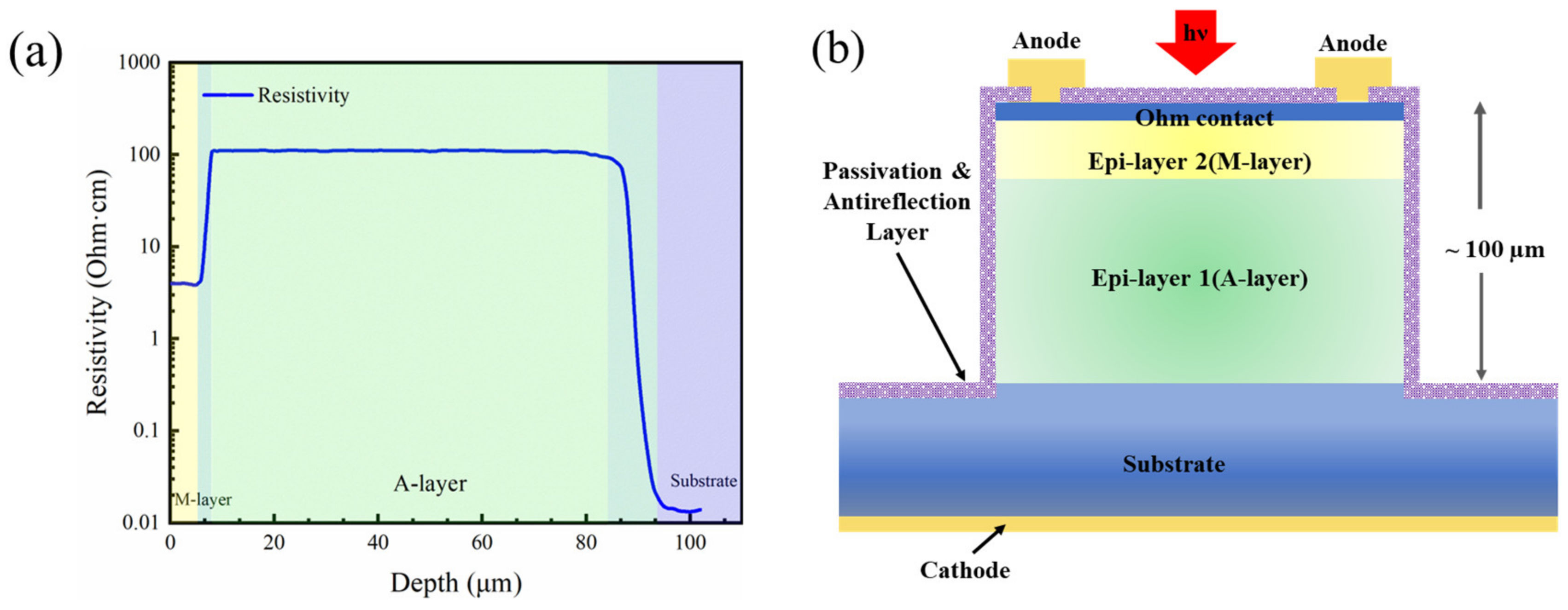
For the design epilayer of the silicon DMSI-APD presented in this work, the traditional separate absorption and multiplication (SAM) structure in the silicon APD is employed. However, unlike previously reported silicon APD fabrication processes, the main working layers in this paper were formed using multiple thick silicon CVD instead of ion implantation and a long-time thermal annealing drive in. Consequently, changes in the epilayer, including doping concentration and thickness, will influence the performance of the fabricated APDs, including dark current, breakdown voltage, and peak responsivity. In a previous study, we simulated the impact of the epi-absorption layer and the epi-multiplication layer on device performance . The spreading resistance profile (SRP) measurement results of the epitaxial wafer are depicted in Figure 1a, while Figure 1b presents the cross-section schematic of the fabricated DMSI-APD. The device epilayer consists of an epi-absorption layer (A-layer) and a multiplication layer (M-layer), which are grown on a low-resistivity substrate using CVD technology. The A-layer and M-layer have a doping concentration and thickness of 1 × 1014 cm−3 , 85 µm, 3.5 × 1015 cm−3 , and 5 µm, respectively. All of these working layers were grown at 800~1000 ◦C. Furthermore, the thickness of the doping gradient layer from the substrate to the absorption layer and from the absorption layer to the multiplication layer is 10 µm and 2 µm, respectively, as shown in Figure 1a.

Figure 1. (a) Spreading resistance profile (SRP) of grown epitaxial wafers. (b) The structure crosssection of the ultra-deep mesa-structure silicon APD.
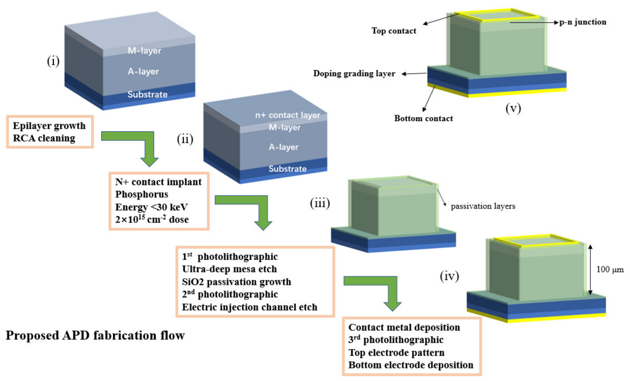
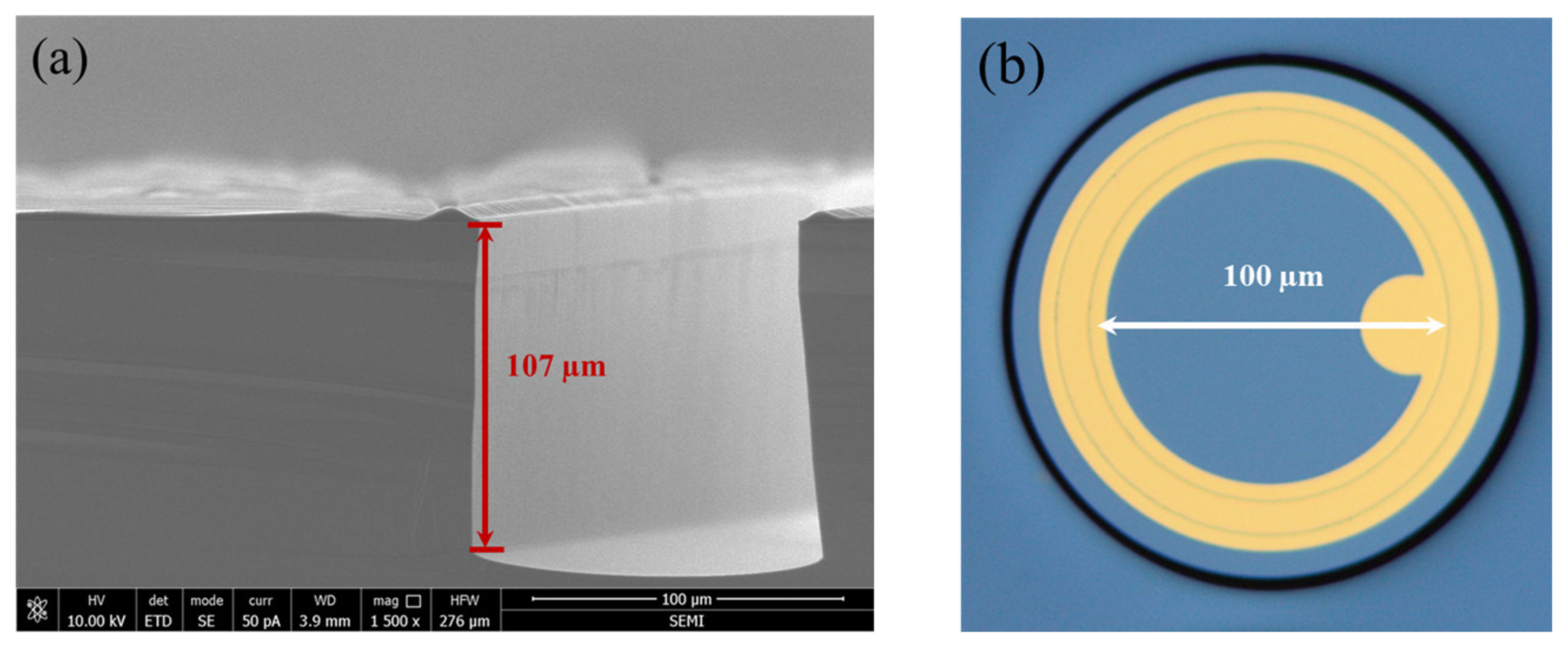
To elucidate the fabrication process of the device more clearly, the improved ultraconcise process flow is shown in Figure 2. The fabrication consisted of four main steps. First, the epi-wafer was cleaned using buffered oxide etch to remove the natural oxide layer from the surface of the grown wafer (step (i) in Figure 2), followed by standard silicon wafer cleaning processes (organic reagents as well as strong acid reagents). Second, the p–n junction was formed through low-energy phosphorus implantation at 30 keV with a dose of 2 × 1015 cm−2 (step (ii) in Figure 2). Afterwards, the implanted dopants were activated and the implantation damage was repaired through rapid thermal annealing (RTA) with annealing parameters of 1050 ◦C for 60 s. Third, the first photolithography was performed and the ultra-deep mesa was etched using inductively coupled plasma (ICP) etching, resulting in a mesa depth of approximately 107 µm, as shown in Figure 3a. In addition, the etching gas was C4F8 and S6F (flow ratio 1:1.2) and the etching temperature was 180 ◦C, the ICP etch rate was around 0.5 µm/cycle, and a total of 200 cycles were performed in the etch process. Next, the dry etched mesa sidewalls were passivated with silicon dioxide (SiO2), dry-oxidized for 2 h, and wet-oxidized for 15 min at 1050 ◦C and 600 ◦C, respectively (step (iii) in Figure 2). Fifth, the second photolithography was completed and an electric injection channel was etched out, followed by the deposition and patterning of Ti/Au alloy to form the metal pads. Finally, the third photolithography was finished and another Ti/Au alloy contact was deposited after chemical–mechanical polishing (CMP) on the backside (step (iv) in Figure 2). Figure 2 (v) and Figure 3b show the three-dimensional (3D)-rendered illustration and the final optical microscopy image of the fabricated DMSI-APD, respectively. Figure 3a also shows the etch profile of the device, with an etch depth of about 107 µm for the mesa, from which it can be seen that the sidewall is about 90◦ steep, with a good etch sidewall roughness. The top table surface in Figure 3b is the active region of the device, and the inside of the metal ring is the photosensitive surface of the device. The shadows around the active region in Figure 3b are due to the significant drop in device height. Compared with other existing silicon APD fabrication processes, the proposed whole fabrication process of the improved DMSI-APD requires only three steps of standard contact UV lithography, and furthermore, the active region is formed with just one low-energy (<30 keV) ion implantation step and rapid thermal annealing. The method exhibits much potential for reducing the fabrication time and steps, and lowering the manufacturing costs, especially ion implantation costs.

Figure 2. Fabrication process flow of the ultra-deep mesa silicon APD. The etched mesa sidewall was passivated with silicon dioxide (SiO2 ), which was grown through dry oxidizing followed by a wet oxidizing process at temperatures of 1050 ◦C and 600 ◦C, respectively. (i) Epitaxial wafer after growth; (ii) Wafer after phosphorus ion implantation; (iii) Wafer after mesa etch and oxide passivation; (iv) Wafer after metal deposition and lift-off; (v) Final fabricated device.

Figure 3. (a) Scanning electron microscope image of etched deep-mesa sidewall of the ultra-deep mesa-structure silicon APD. (b) Optical microscopy image of fabricated ultra-deep mesa-structure silicon APD.
3. Device Characterization and Discussion
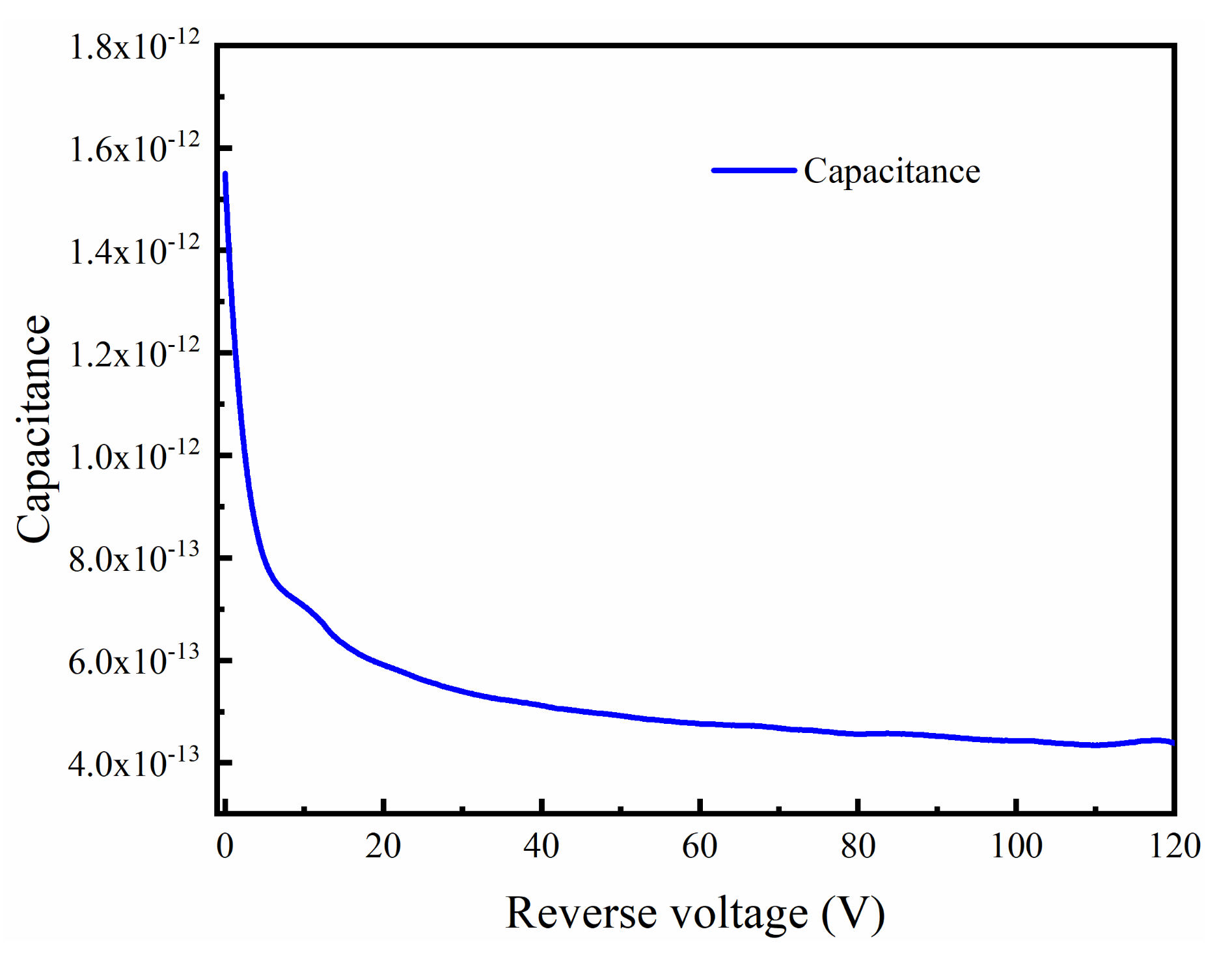
The capacitance, as a function of reverse voltage, was measured and the rise time was calculated for the DMSI-APD device. Figure 6 illustrates the measured capacitance at various reverse voltages, with a measurement frequency of 1 MHz and a voltage step of 0.5 V. The results show a significant decrease in capacitance as the reverse voltage increased, and at the punch-through voltage state, the capacitance was below 500 fF, which was lower than that of most products, such as the Hamamatsu S14645 series. The main reason for the low capacitance is that the device depletion region is thicker and no additional parasitic capacitance was introduced after preparation, which also contributed to lowering the RC time constant of the device.

Figure 4. Capacitance versus reverse voltage of fabricated DMSI-APD
4. Conclusions
In this work, an ultra-deep mesa-structure silicon APD with an improved concise fabrication process was proposed and fabricated. The improved process exhibited reduced complexity, with the number of photolithography and ion implantation steps being reduced by at least half of those involved in the existing process. Furthermore, only one low-energy ion implantation (below 30 keV) was implemented for the whole fabrication process. The fabricated ultra-deep mesa-structure silicon APD showed a 140 V breakdown voltage, a dark current below 1 nA, a maximum gain exceeding 1000, and a high responsivity of 103 A/W@870 nm. Moreover, the device has a low capacitance of 500 fF, consequently yielding a rapid optical pulse response time shorter than 2.7 ns at 55 V reverse voltage.
Limited by the sidewall roughness and defects introduced by the present etching, the dry oxidation time used was not long enough, which resulted in the defects and damage not being completely suppressed, thus causing the dark current of the device to fail to reach the desired value. In addition, due to the long etching time, the device also has high requirements for etching uniformity and repeatability, which are several optimizable points that we intend to continue to solve in our future work. After these issues are subsequently resolved, the proposed device will exhibit much potential for reducing the fabrication time and steps, and lowering the manufacturing costs, especially the ion implantation costs associated with weak light detection.