Abstract — High-temperature operation of the p-GaN gate high-electron-mobility transistor (HEMT) was investigated, specifically up to 500 °C. The p-GaN gate HEMT demonstrated stable behavior with normally-off operation, steep increase of drain current in the subthreshold region, and suppressed off-state current. By adding Al2O3 etch-stop layer, the device showed significant reduction in subthreshold swing when measured at 500 °C, effectively mitigating hysteresis in the transfer characteristics. Additionally, the lifetime of the gate stack with the etch-stop layer was estimated to be much longer than that of the stack without the etch-stop layer. Through the integration of the depletion-mode (D-mode) metalinsulator-semiconductor HEMT (MIS-HEMT) device with the p-GaN gate device, a direct-coupled field-effect transistor logic (DCFL) inverter was fabricated. This inverter showed stable logic operation up to 500 °C, featuring rail-to-rail operation and large gain. A long-term reliability test conducted at 500 °C for 100 hours revealed stabilized onstate and off-state values after about 50 hours of operation.
AlGaN/GaN Schottky HEMTs have been tested for high temperature electronics, but gate metal diffusion into the barrier layer and large gate leakage severely degraded device characteristics at high temperatures . MIS-HEMT devices, with gate dielectric layer between the gate metal and AlGaN barrier, showed potential for reducing gate leakage current and improving gate stack stability. However, achieving stable high temperature operation with MIS-HEMT structures has been challenging due to threshold voltage instability caused by AlGaN strain relaxation and interface traps . Most studies have focused on operation up to 200 °C, whereas industry applications often require higher temperatures. Furthermore, there is limited research on normally-off high temperature HEMTs, which are more practical and versatile for real-world applications.
II. DEVICE FABRICATION
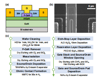
The p-GaN gate HEMT device was fabricated on the pGaN/AlGaN/GaN heterostructure grown on silicon substrate. The substrate consists of 70 nm p-GaN, 15 nm Al0.2Ga0.8N, 0.7 nm AlN, 200 nm unintentionally doped GaN, 5.8 µm GaN buffer, and silicon substrate from top to bottom. The schematic of the device is shown in Fig. 1(a), and the top-view scanning electron microscopy (SEM) image of the fabricated device is shown in Fig. 1(b). The length of gate electrode/p-GaN contact area was 1.5 µm , and the width was designed to be slightly smaller than the width of the mesa-isolated AlGaN/GaN block to prevent the electrodes from directly contacting the sidewall, which may have dry etching induced damage. The fabrication process is shown in Fig. 1(c). The p-GaN layer on top of the substrate was removed, and mesa isolation was carried out by dry etching performed using inductively coupled plasma reactive ion etching (ICP-RIE) with Cl2 and BCl3. Ti/Al/Ni/Au (20 nm/120 nm/60 nm/ 50 nm) stack was then deposited as the source/drain electrode using e-beam evaporator, followed by rapid thermal annealing at 900 °C for 30 seconds in N2 to form the ohmic contact. 10 nm of Al2O3 etch-stop layer was deposited using atomic layer deposition (ALD), and 200 nm of Si3N4 layer was deposited using plasma-enhanced chemical vapor deposition (PECVD). Gate stack and source/drain contact windows were opened by ICP-RIE using SF6, and the ALD Al2O3 etch-stop layer was removed by wet etching using buffered oxide etch (BOE). Ni/Au (50 nm/150 nm) layer was deposited as the gate electrode using the e-beam evaporator, and post-metallization annealing was performed at 500 °C for 5 minutes in N2.

Fig. 1. (a) Schematic of a p-GaN gate HEMT. (b) SEM image of the pGaN gate HEMT device. (LG = 4 µm, LGS = 4 µm, LGD = 9 µm, W = 100 µm) (c) Fabrication process of the p-GaN gate HEMT.
III. RESULTS AND DISCUSSION
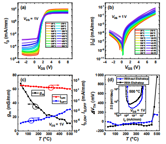
Temperature dependence of the transfer characteristic and gate leakage current of p-GaN gate HEMT with etch-stop layer are shown in Fig. 2(a) and 2(b), respectively. For the high temperature measurements, the device was measured in vacuum environment, with contact made using probe tips. The gate voltage was increased and decreased in steps of 0.1 V, with time interval of approximately 0.2 seconds between each gate voltage value, and there was no delay introduced between the forward and backward sweeps. The device showed stable high temperature operation with suppressed off-state current and sharp subthreshold slope. Normally-off operation was maintained with slight threshold voltage shift towards the negative direction, from 1.4 V at 25 °C to 0.9 V at 500 °C, estimated by the gate bias at which the drain current is 10- 2 mA/mm. The gate leakage current gradually increased with increasing temperature, but the gate stack demonstrated stable operation without breakdown, even with large gate bias of 8 V up to 500 °C. Fig. 2(c) shows temperature dependence of the on-state current, off-state current, and peak transconductance. As the temperature increases, the on-state current gradually decreased, off-state current gradually increased, and the transconductance decreased. As the temperature increases, the mobility of the channel formed at the AlGaN/GaN interface decreases primarily due to increased phonon scattering, leading to a decrease in the on-state current and transconductance. The off-state drain current can be attributed to the carrier hopping current flowing through the dry etching induced traps on the AlGaN and GaN surfaces, which can be further suppressed by optimizing the dry etching recipe.

Fig. 2. (a) Transfer characteristic and (b) gate leakage current of a pGaN gate HEMT with etch-stop layer at various temperatures up to 500 °C. (c) Temperature dependence of the peak transconductance (gm), on-state current at VGS = 5 V, and off-state current at VGS = 0 V. (d) VTH hysteresis (∆VTH) of the transfer curve with VGS sweep range of -3 V ~ 8 V measured at various temperatures for the p-GaN gate HEMT with and without the etch-stop layer. Here, VTH hysteresis was extracted as ∆VTH = VTH–F – VTH–B where VTH–F is the threshold voltage in the forward sweep and VTH–B is the threshold voltage in the backward sweep. Inset shows subthreshold swing (SS) of the p-GaN gate HEMT with and without the etch-stop layer at 500 °C.
III. RESULTS AND DISCUSSION
Temperature dependence of the transfer characteristic and gate leakage current of p-GaN gate HEMT with etch-stop layer are shown in Fig. 2(a) and 2(b), respectively. For the high temperature measurements, the device was measured in vacuum environment, with contact made using probe tips. The gate voltage was increased and decreased in steps of 0.1 V, with time interval of approximately 0.2 seconds between each gate voltage value, and there was no delay introduced between the forward and backward sweeps. The device showed stable high temperature operation with suppressed off-state current and sharp subthreshold slope. Normally-off operation was maintained with slight threshold voltage shift towards the negative direction, from 1.4 V at 25 °C to 0.9 V at 500 °C, estimated by the gate bias at which the drain current is 10- 2 mA/mm. The gate leakage current gradually increased with increasing temperature, but the gate stack demonstrated stable operation without breakdown, even with large gate bias of 8 V up to 500 °C. Fig. 2(c) shows temperature dependence of the on-state current, off-state current, and peak transconductance. As the temperature increases, the on-state current gradually decreased, off-state current gradually increased, and the transconductance decreased. As the temperature increases, the mobility of the channel formed at the AlGaN/GaN interface decreases primarily due to increased phonon scattering, leading to a decrease in the on-state current and transconductance. The off-state drain current can be attributed to the carrier hopping current flowing through the dry etching induced traps on the AlGaN and GaN surfaces, which can be further suppressed by optimizing the dry etching recipe.
Lifetime of the device was estimated by applying the gate bias on the array of devices with LGS = LGD = 4 µm while source/drain electrodes were grounded. Weibull plots of the time to breakdown (tBD) distribution and lifetime predictions for the devices are shown in Fig. 3(a) and 3(b), indicating lifetime of 10 years for the device without the etch-stop layer at VGS = 4.3 V, and lifetime of 10 years for the device with the etch-stop layer at VGS = 5.9 V. Therefore, the addition of the etch-stop layer, which serves to protect the p-GaN surface, significantly improves the lifetime of the gate stack, highlighting the importance of preserving the intact p-GaN interface.
IV. CONCLUSION
In summary, the p-GaN gate HEMT with the etch-stop layer demonstrated stable operation up to 500 °C, and long-term reliability was further confirmed by the consistent performance observed during 100 hours of device characterization at this temperature. By utilizing the etch-stop layer to preserve the intact p-GaN surface and avoiding direct contact of the gate electrode on the mesa sidewall, the device showed suppressed off-state current, steep subthreshold slope, and improved hysteresis. Additionally, long-term reliability test confirmed reasonably long device lifetime with appropriate supply voltage, and stable high temperature operation of the DCFL inverter was also examined. We believe that this p-GaN gate device with the etch-stop layer is a strong candidate for high temperature logic device, opening another path for development of high temperature electronics.