Abstract: We design, fabricate, and demonstrate a low-loss and broadband optical interposer with high misalignment tolerance for large-scale integration of many chips using thermal compression flip-chip bonding. The optical interposer achieves flip-chip integration with photonic integrated circuit die containing evanescent couplers with inter-chip coupling loss of 0.54dB and ±3.53µm 3-dB misalignment tolerance. The loss measurement spectrum indicated wavelength-insensitive loss across O-band and C-band with negligible spectral dependence. Further, we demonstrate 1 to 100 wafer-scale equal power splitting using equal power splitters (EPS) and a path length matching design fabricated using a wafer-scale fabrication technique.
1. Introduction
The explosive growing demands for sensing, optical computing, and data communication require large-scale and energy-efficient electro-optics integrated photonics systems, while the integration difficulty, cost, and yield limit the size and function of a single chip. Therefore, co-packaged multi-chip integration is investigated to improve performance and capabilities. Optical interposer supporting many function blocks with electrical and optical connection brings solutions for complex electro-optics integrated systems, such as large-scale light detection and ranging (LIDAR) with wide emitting apertures, and high-performance computing (HPC) systems assisted by optical interconnects. Such systems demand the optical interposer to realize large-scale, high integration density, high throughput, high energy efficiency, and simplicity in packaging.
A critical component in the optical interposer is the inter-chip coupler, which couples light between the interposer and photonic chips to support a high-efficiency signal transfer between the photonic chips under achievable packaging quality, with enough bandwidth to support the desired applications. Inter-chip couplers based on gratings typically suffer from a high coupling loss and/or narrow bandwidth. Polymer waveguides offer a low-loss and broadband inter-chip coupler solution at the cost of relatively low reliability and temperature tolerance. The silicon nitride(Si3N4) platform serves as an excellent candidate for the optical interposer because it enables low-loss and broadband transition for compact inter-chip coupling thanks to the low index contrasts between the core and cladding material. In this work, photonic integrated circuits(PICs) are flip-chip bonded onto the optical interposer using a thermal compression bonding process during packaging with an optical connection enabled by the inter-chip couplers. Meanwhile, the two bonded pads maintain the electric connection.
2. Low-loss broadband inter-chip coupler design
A conventional flip-chip bonding process can achieve a ±0.5µm misalignment after placement, which could significantly increase after the bonding. The optical coupling efficiency could be impaired under such misalignment. Thus, our design aim is to minimize the inter-chip coupling loss under an achievable post-bonding misalignment.
We use the wavelength-insensitive evanescent coupling on the Si3N4 platform to efficiently couple between chips. We utilize its low propagation loss, large transparency window, and large mode size, brought by the low refractive index contrast on Si3N4/SiO2 waveguides. We design a low-loss broadband inter-chip coupler using a pair of Si3N4 inversed tapers embedded in SiO2 cladding for optical transmission. We use metals at the surface of the chips for bonding, alignment, and electrical connection, as presented in Fig. 1(a). During transmission, the optical beam transmitted in one Si3N4 waveguide is expanded by the inversed taper and coupled to the other taper evanescently. Figure 5 shows the evolution of the mode profile during transmission. The simulation uses a pair of inversed tapers with 500nm cladding on both sides and a 200nm air gap in between. The optical signal incident from the bottom left in Fig. 5(a) transmits across the airgap and is coupled into the upper inversed taper. We performed Au-to-Au flip-chip thermal compression bonding to package the silicon photonics chips to the interposer guided by the alignment marks on the Au layers.
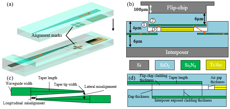
Fig. 1. (a) Schematic of the inter-chip coupler. Alignment marks and bonding pads are on the surface of the two chips. The orange arrows denote the beam propagation direction. The black arrow denotes the chip movement direction during flip-chip bonding. (b) Diagram of the flip-chip and Interposer packaging. The numbers denote (1) scattering loss at the edge of the air trench, (2) scattering loss at the edge of the flip-chip, and (3) coupling loss. (c) Top view and (d) side view diagram of the inter-chip coupler.
We design a test structure with straight waveguides to measure the coupling loss of the inter-chip coupler, as shown in Fig. 1(b). The inter-chip coupler has a >50µm longitudinal misalignment (presented in Fig. 1(c)) tolerance, so only lateral misalignment is considered in this work. The test structure includes an array of the inter-chip coupler with a variable lateral offset to measure the coupling loss and the misalignment tolerance. The top cladding thickness was reduced to around 500nm at the coupling region to enhance the coupling efficiency. The flip-chip is plugged into the trench on the interposer during packaging. We adopt a 100nm silicon nitride thickness and a 1000µm taper length as a trade-off between the misalignment tolerance and device footprint. The total optical loss between the interposer and the flip-chip comes from the optical scattering and optical coupling. Optical mode discontinuity causes scattering loss during optical transmission. There are two discontinuities when the optical signal transmits on the waveguides on the interposer: (1) the edge of the air trench on the interposer, and (2) the edge of the flip-chip, and hence introduce the air trench scattering loss and the flip-chip scattering loss, as shown in Fig. 2(d) with blue and red dashed line box, respectively. Figure 2(a) and (b) show reference waveguides for measuring the scattering loss and the coupling loss, which are both straight waveguides, while the waveguide in (b) goes through two times of scattering. Scattering loss induced by mode discontinuity (as shown in Fig. 4(a-c)) decreases while increasing the interposer exposed cladding thickness and the air gap thickness (shown in Fig. 1(d)). The simulated scattering loss in Fig. 3(a) indicates that the scattering loss at the edge of the air trench dominates the total scattering loss. Figure 3(b) indicates the misalignment tolerance increase with the increase of the taper length. We design a 500nm interposer exposed cladding thickness and a less than 100nm flip-chip cladding thickness as a trade-off between the total inter-chip loss and lateral misalignment tolerance. The waveguide width is 3µm, and the tip width of all the inversed tapers is 250nm, limited by the minimum feature size of our ASMLTM PAS 5500 300 deep-UV lithography stepper. The air gap thickness is mainly determined by the sum of the two metal thicknesses on the chips. During bonding and annealing, the two metal pads will be squeezed together, making the gap thickness lower than the sum of the metal thicknesses. The two bonded metal pads enable electrical connections between the bonded chips and the interposer.
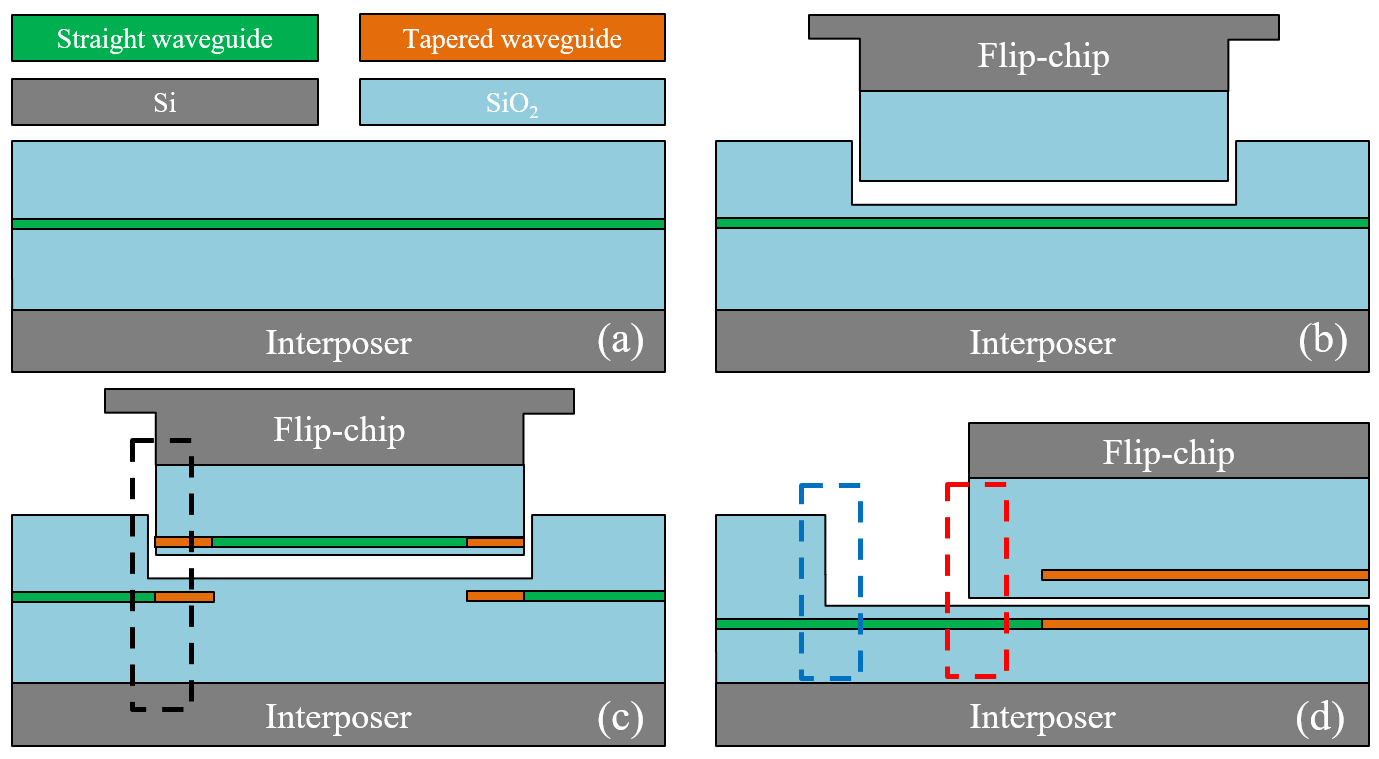
Fig. 2. (a) Reference waveguide, (b) reference waveguide with scattering loss, (c)waveguide with scattering loss and coupling loss, and (d) zoom-in view of the black dashed line box in (c). The blue and red dashed line contains the interface that induces the air-trench scattering loss and the flip-scattering loss.
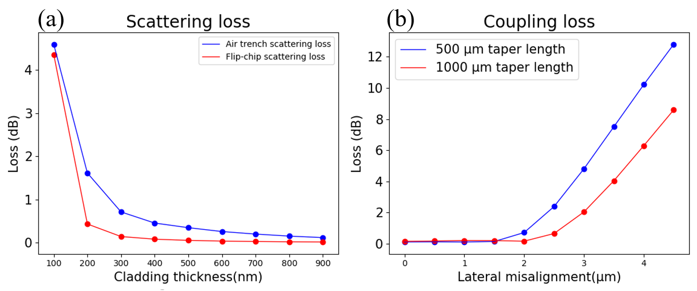
Fig. 3. (a) Simulated scattering loss at the edge of the air trench and flip-chip as a function of bottom cladding thickness. The air gap thickness is 200nm. (b) Simulated coupling loss as a function of lateral misalignment. The gap thickness is 800nm, and the air gap thickness is 200nm,
3. Device fabrication
Figure 4(a-m) shows the fabrication flow chart of our interposer and the flip-chip. The interposer and the fabrication start with an initial wafer cleaning on a 150mm silicon wafer using a 120◦C piranha solution. We perform wet oxidation under 1050◦C to get a 6µm SiO2 bottom cladding. We then deposited stoichiometric Si3N4 using low-pressure chemical vapor deposition (LPCVD). The interposer and flip-chip waveguide design is patterned onto the Si3N4 layer using deep-UV lithography and etching, as presented in Fig. 4(r). We deposited a 4µm low-temperature oxide (LTO) on the interposer wafer using LPCVD as the top cladding, followed by a chemical mechanical polishing (CMP) . The polished surface has an average surface roughness of 0.2nm, measured by atomic force microscopy (AFM), as shown in Fig. 4(q). We etch the trench on the interposer using inductively coupled plasma (ICP) etching with low surface damage since the roughness on the trench surface will induce scattering loss because of local discontinuity. After etching, the surface roughness is 0.5nm, as shown in Fig. 4(p). The surface roughness on the two surfaces will induce scattering and increase the coupling loss. On the flip-chip, we deposit a 350nm LTO on top of the patterned Si3N4 layer, and we remove 250nm LTO by CMP to ensure the flip-chip cladding thickness is around 100nm. Using lift-off, we patterned 20nm Ti and 80nm Au on top of the interposer and the flip-chip wafers. Figure 4(n) and (o) present the alignment mark microscope photos on the interposer and the flip-chip, respectively. We perform a SiO2/Si deep etching process to make the flip-chip accommodated by the trench on the interposer during packaging and expose the edge of the waveguides on the interposer chip. Figure 4(s) shows the microscope photo of the tapers on the interposer chip after fabrication.
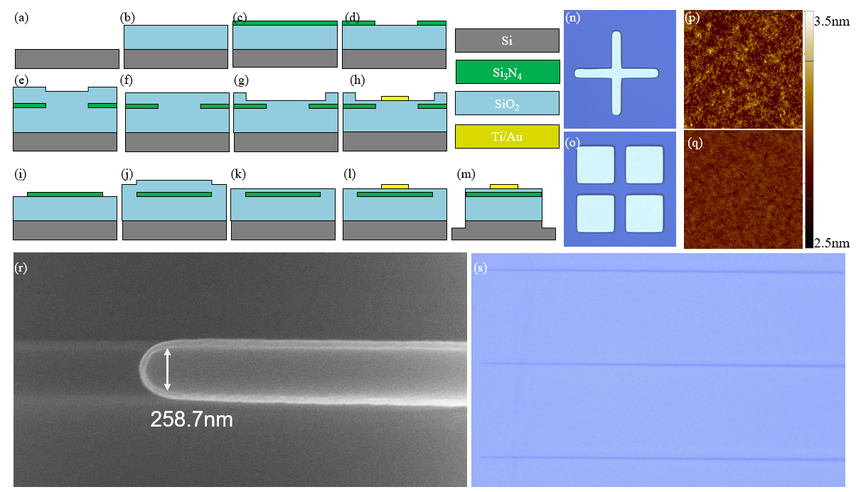
Fig. 4. Fabrication flow chart of (a) initial wafer cleaning; (b) thermal oxidation; (c) Si3N4 deposition; (d) interposer Si3N4 lithography and etching; (e) interposer LTO deposition; (f) interposer CMP; (g) interposer LTO lithography and etching; (h) interposer Ti/Au lift-off; (i) flip-chip Si3N4 lithography and etching; (j) flip-chip LTO deposition; (k) flip-chip CMP; (l) flip-chip Ti/Au lift-off; (m) deep LTO/Silicon etching,(n) and (o) microscope photo of the alignment marks on the interposer and the flip-chip, respectively, (p)AFM measurement of the SiO2 surface inside the LTO trench after step (g), (q) AFM measurement of the SiO2 surface after CMP, (r) SEM photo of a patterned Si3N4 taper, at the tip, and (s) microscope photo of the tapers.
5. Wafer-scale optical power distribution
Complex electrical-optical systems require integrating many components, raising the requirement for large-scale integration. We develop a wafer-scale equal power splitting on the Si3N4 platform to split the input optical power into a 2D 10×10 array with a 1cm period in both directions using the layout shown in Fig. 5(a) at 1550nm wavelength and fundamental TE mode. The round contour shows a 6-inch silicon wafer. The light from an external laser is split and distributed into a 10×10 array using cascaded 1×10 EPSs, with the layout shown in Fig.5(b). The ten outputs from a single EPS are routed as indicated by the port numbers in Fig. 5(a) and (d). We design a wafer-scale optical interposer by placing inversed tapers in Fig. 5(c) at the end of the distribution to support up to 100 dies. As a proof of concept demonstration, we design and fabricate a wafer-scale grating array by replacing the inversed taper with the grating in Fig. 5(c) to observe the light emission from the top.
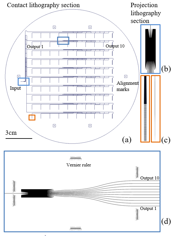
Fig. 5. (a) Layout of a wafer-scale optical interposer using a path length matching and stitching design, blue boxes contain EPSs, and Orange boxes contain gratings or inversed tapers. (b) the layout of the EPS, and (c) the layout of gratings and an inversed taper. (d) Zoom-in view of the centered blue box in (a).
6. Conclusion
We have experimentally demonstrated an optical interposer for multi-chip integration using thermal-compression flip-chip bonding. The interposer uses inter-chip couplers with a 0.77dB scattering loss, 0.54dB coupling loss, and ±3.53µm 3-dB misalignment tolerance, so the total insertion loss is 1.31dB. The inter-chip coupler can achieve less than 1.75dB total insertion loss from 1200nm to 1600nm wavelength. We have designed and fabricated a wafer-scale equal optical power distribution for large-scale integration realized by a wafer-scale fabrication technique. The wafer-scale optical power distribution uses EPSs, a path length matching design, to achieve equal power splitting. We put gratings at the terminal of the distributions to observe the optical power from the top.