Abstract
Graphene nanoelectronics’ potential was limited by the lack of an intrinsic bandgap and attempts to tailor a bandgap either by quantum confinement or by chemical functionalization failed to produce a semiconductor with a large enough band gap and a sufficient mobility. It is well known that by evaporating silicon from commercial electronics grade silicon carbide crystals an epitaxial graphene layer forms on the surfaces . The first epigraphene layer to form on the silicon terminated face, known as the buffer layer, is insulating. It is chemically bonded to the SiC and spectroscopic measurements have identified semiconducting signatures on the microscopic domains. However, the bonding to the SiC is disordered and the mobilities are small. Here we demonstrate a quasi-equilibrium annealing method that produces macroscopic atomically flat terraces covered with a well ordered epigraphene buffer layer that has a 0.6 eV bandgap. Room temperature mobilities exceed 5000 cm2 /Vs which is much larger than silicon and 20 times larger than the phonon scattering imposed limit of current 2D semiconductors. Critical for nanotechnology, its lattice is aligned with the SiC substrate, it is chemically, mechanically, and thermally robust, and it can be conventionally patterned and seamlessly connected to semimetallic epigraphene making semiconducting epigraphene ideally suited for nanoelectronics.
Main
The graphene revolution was originally driven by the search for new electronic materials that could succeed silicon. Graphene, which is a semimetal (i.e., a gapless semiconductor) was a likely candidate following predictions that, due to quantum confinement, graphene nanoribbons can be semiconductors. Efforts to produce high quality semiconducting ribbons were not successful, so research focused on altering the electronic structure of graphene chemically to produce a viable semiconductor. However, these efforts also had limited success and interest shifted away from graphene towards 2D materials that are intrinsically semiconducting. Here we show that well-annealed graphene on a specific silicon carbide crystal face is an extremely high mobility 2D semiconductor.
SEG production
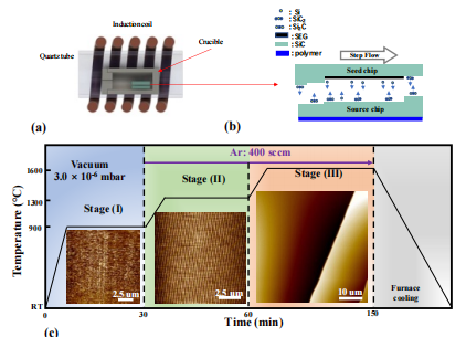
Conventional epigraphene and buffer layer is grown in a confinement-controlled sublimation (CCS) furnace (Fig 1a-b) where a 3.5 mm x 4.5 mm semi-insulating SiC chip is annealed in a cylindrical graphite crucible in a 1 bar Ar atmosphere at temperatures ranging from 1300 C to 1600 C (Fig. 1c). The crucible is supplied with a small leak. The rate silicon escapes from the crucible determines the rate at which graphene forms on the surface. In this way, the growth temperature and the graphene formation rates are controlled.

Fig. 1 SEG produc+on, (a) Schema+c diagram of a CCS furnace with two 3.5 mm x 4.5 mm SiC chips inside a closed cylindrical graphite crucible that is supplied with a leak inside a quartz tube. The crucible is induc+vely heated by high frequency currents through a coil. (b) The two chips are stacked with the C-face of the boIom chip (Source) facing the Si-face of the top chip (Seed). At high temperatures a slight temperature difference between the chips causes a net mass flow from the boIom chip to the top chip resul+ng in the growth of large terraces on the seed chip by step flow growth on which a uniform SEG film grows. (c) SEG is grown in three stages. In stage (I) in vacuum the chip is heated to 900 C for about 25 min to the surface; Hea+ng to 1300 C for about 25 min. 1 bar of Ar produces a regular array of bilayer SiC steps and ≈ 0.2 µm wide terraces. SEG coated (0001) terraces grow in Stage (III) at 1600 C in 1 bar of Ar step bunching and step flow produce large atomically flat terraces on which a buffer layer grows in quasi-equilibrium condi+ons established between the C-face and the Si-face. The large SEG coated (0001) terraces are explained in terms of its very large stability.
If the leak is sealed, then graphene growth is strongly suppressed. Graphene growth is further suppressed in the so-called sandwich or face-to-face method (Sup Mat), where two chips are stacked, typically with the Si-face of one chip facing the Si-face of the other. In 1 bar of Ar, virtually no silicon can diffuse out of the micron scale gap between the chips so that the 1:1 Si:C ratio is maintained, even at high temperatures where the Si evaporation rates from the surfaces are high. Under these conditions significant step flow and step bunching is observed (Fig 1c). Step bunching is the process where substrate surface steps due to the unavoidable slight miscut of the crystal which is nominally cut along the (0001) face, merge to produce large atomically flat (0001) terraces bounded by proportionally high steps.
SEG characterization
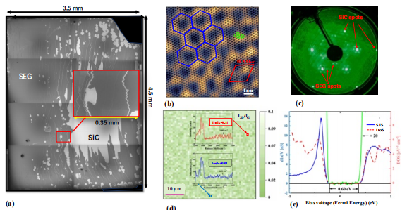
SEG is investigated on all relevant length scales. On the 100 nm to the 1 mm scale, scanning electron microscopy (SEM) can provide a high contrast that distinguishes bare SiC, SEG and graphene (Fig. 2a). On the nanometer scale, graphene and SEG are also readily identified in scanning tunneling microscopy (STM) by its SiC6x6 modulation (Fig. 2b). Low energy electron diffraction (LEED) is used to identify SEG and to verify its atomic registration with the SiC substrate (Fig 2c). LEED is also used to distinguish SEG from graphene. Raman spectroscopy (1 µm to 100 µm) is very sensitive to graphene and SEG, and traces of graphene are easily identified by its intense characteristic 2D peak (Fig. 2c). Lateral force microscopy (LFM) distinguishes SEG from SiC and graphene in micron scale scans. Atomic force microscopy (AFM), SEM and optical microscopy can identify surface steps. AFM is used to measure the amplitude of the steps (Fig. 6). Using a combination of these probes we find that in a wide range of production temperatures graphene is absent to any detectible level, even on substrate steps where it is readily formed in the conventional CCS method. Figure 2e shows cryogenic scanning tunneling spectroscopy which maps the density of states (DoS) of SEG as a function of the Fermi energy. The image shows a well-defined band gap of 0.6 eV. There are no detectible states in the band gap in contrast to buffer layer samples produced by conventional sublimation methods.

Fig. 2 SEG characteriza+on demonstra+ng high coverage of well-ordered, graphene free, crystallographic aligned SEG, with a well-defined bandgap. (a) Composite electron microscope image of a full 3.5 mm x 4.5 mm wafer. The SEM is tuned to provide a vivid contrast between SiC (white areas) and SEG (grey areas). Approximately 80% of the surface is covered with SEG. Graphene would show up as very dark patches (the black spots seen here are dust par+cles). The largest step-free areas are about 0.5 mm by 0.3 mm. (b) Low temperature, atomic resolu+on STM image of SEG showing the graphene honeycomb la\ce (green) that is spa+ally modulated with a (6x6)SiC super-periodic structure (red rhombus; purple hexagons) that corresponds to the SEG height modula+on due to the covalent bonding to the substrate. (c) LEED of SEG showing the characteris+c 6√3x6√3R30° diffrac+on paIern of the SEG la\ce, which reveals its graphene-crystal structure and the crystallographic alignment of the SEG with respect with the SiC substrate atoms. There is no trace of graphene which is invariably abundant in conven+onally produced buffer layer samples. (d) Raman map of a 50 µm by 50 µm area with a 1 µm resolu+on measuring the intensity ra+o I2D/IG of the intensity at 2680 cm-1 and at 1620 cm-1 . For graphene I2D/IG ≈ 2. The red arrow corresponds to the red spectrum taken at the spot where the intensity ra+o is the largest in the 2500 spectra in the map demonstra+ng the absence of any graphene on the surface as confirmed with other probes. (e) Low temperature STS of SEG, showing the 0.6 eV band gap of SEG (blue line) compared with the calculated DoS of SEG (red dashed line). There is no measurable intensity in the gap indica+ng a low density of impurity states.
SEG transport properties
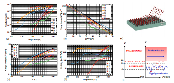
A series of transport measurements on SEG Hall bars that were patterned using two different methods. The samples were p-doped in ambient air in pure oxygen or in pure O2, and with ultraviolet (UV) radiation. In this way room temperature charge densities n from n=4x1012 cm-2 to 4x1013cm-2 were achieved. We are specifically interested in oxygen doping because it significantly p dopes the buffer layer (and SEG) and it is the only atmospheric gas that is stably absorbed on the buffer layer as was demonstrated by Turmaud ; annealing at 400 C in vacuum is required to desorb the oxygen (see also Sup. Mat).

Fig3
The conductivities of the samples (Fig. 3a) all show a monotonic increase with increasing temperature. The room temperature conductivities range from 1 to 8 x 10⁻³ S corresponding to resistivities r from 125 W to 330 W. The low temperature values are up to a factor of 1000 smaller. Charge densities (Fig. 2b) range from ≈0. 2 x 1012 cm-2 - 40 x 1012 cm-2 . The STS measurements (Fig. 2a) show that SEG is intrinsically charge neutral, so that the charging is caused by environmental gasses (including trace volatile organic compounds) and by residual resist from lithographic processing. The mobility (Fig. 2c) generally increases with increasing temperature tending to saturate at higher temperatures. The maximum measured mobility is 5500 cm2 V-1 s-1 . The room temperature SEG conductivities, charge densities and mobilities are all within ranges that are typical for epigraphene. However, the temperature dependences are reminiscent of a doped semiconductor with deep acceptor states as elaborated below.
Conclusion and perspective
The singular focus of epigraphene nanoelectronics research, even predating mainstream graphene research, was to develop a 2D nanoelectronics platform to succeed silicon electronics. Graphene’s lack of a band gap was universally considered to be the major hurdle towards this goal. Here we have demonstrated that a well crystallized epigraphene buffer layer is an excellent 2D semiconductor with a 0.6 eV band gap and with room temperature mobilities that greatly surpass all current 2D semiconductors. A prototype FET has an on-to-off ratio of 104 which may reach 106 in optimized devices.
METHODS
Sample Production
Samples used for transport measurements were produced in a closed cylindrical high purity graphite crucible, 14 mm long and 10 mm in diameter with a cylindrical bore of 5.5 mm. The crucible is closed and supplied with a cap, that is perforated with a 1 mm hole (Fig.1a). The crucible is placed in a quartz tube and heated inductively. The temperatures are monitored and controlled with an optical pyrometer. The typical sandwich is composed of two 3.5x4.5 mm SiC chips, where the Si-face of the top chip (the seed chip) faces the C-face of the bottom chip (the source chip). The Si-face of the source chip (i.e. specifically not between the chips) may be coated with a polymer which most likely causes its temperature to slightly increase relative to the top chip.

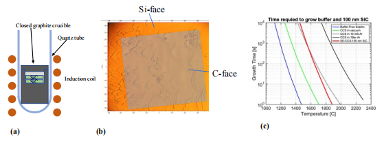
Fig. 5 (a) Vertical furnace with improved temperature gradient control. (b) Overlapped images of the surface of a Siface seed chip and mirror image of the corresponding C-face source chip (slightly shifted) showing identical complementary topological features, i.e. material removed from the C-face is deposited directly above it on the Siface which demonstrates the close interaction between the two chips. (c) Approximate times to grow a buffer layer and to grow 100 nm SiC from the source chip on the seed chip where the former is more than 10 C cooler than the latter.
The graphitized polymer helps to establish the required temperature differential between the top and the bottom chip. However, entirely similar results have also been obtained without the polymer coating (i.e. Fig. 2e) in a vertical furnace (Fig 5a) in which the temperature gradient is controlled by the location of the sandwich in the crucible. A specific temperature difference within the relatively narrow annealing temperature window is found to be important. While nominally, the C face of the bottom chip is free of graphene, it becomes fully covered with graphene, with certain polymer coatings (Sup Mat). The Si face of the top chip always has a buffer layer covering step free terraces; however coverage is not always complete, especially in the middle of the chip. This may be due to a slightly increased Si vapor pressure there. The size of the terraces and buffer layer coverage vary considerably depending on temperatures and annealing times, polymer coating, SiC doping, SiC polytypes, and miscut size and direction. Current research focuses on optimizing these parameters, as well as developing alternative crucible designs in which the temperature gradient is better controlled, and with chips supplied with corrals that define growth areas.
Figure 5 (a) shows an alternative crucible design to study the effects of the temperature gradient where the gradient increases from the middle to the top of the crucible, as demonstrated in numerical simulations of the temperatures. This configuration is also used to demonstrate the mass transport from the hotter source chip to the cooler seed chip. For example, figure 5 (b) shows optical images of the surfaces of the Si-face seed chip superimposed with a mirror image of the Cface source chip, which clearly shows that their complementary nature, that is, material which is removed from the hotter C-face chip is deposited on the cooler Si-face chip. The C-face image has been shifted slightly for clarity. We also find that when the temperature gradient is inverted making the Si-face chip the seed source chip and the C-face chip the seed chip, then we find that the Siface is covered with SEG but the (0001) terraces are small.
下一篇: 碳纳米管集成电路技术的路线图和技术挑战