Silicon photonics has developed into a mainstream technology driven by advances in optical communications. The current generation has led to a proliferation of integrated photonic devices from thousands to millionsmainly in the form of communication transceivers for data centers. Products in many exciting applications, such as sensing and computing, are around the corner. What will it take to increase the proliferation of silicon photonics from millions to billions of units shipped What will the next generation of silicon photonics look like? What are the common threads in the integration and fabrication bottlenecks that silicon photonic applications face, and which emerging technologies can solve them. This perspective article is an attempt to answer such questions. We chart the generational trends in silicon photonics technology, drawing parallels from the generational definitions of CMOS technology. We identify the crucial challenges that must be solved to make giant strides in CMOS-foundry-compatible devices, circuits, integration, and packaging. We identify challenges critical to the next generation of systems and applications—in communication, signal processing, and sensing. By identifying and summarizing such challenges and opportunities, we aim to stimulate further research on devices, circuits, and systems for the silicon photonics ecosystem.
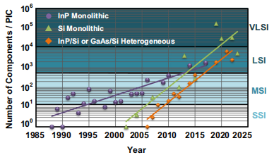
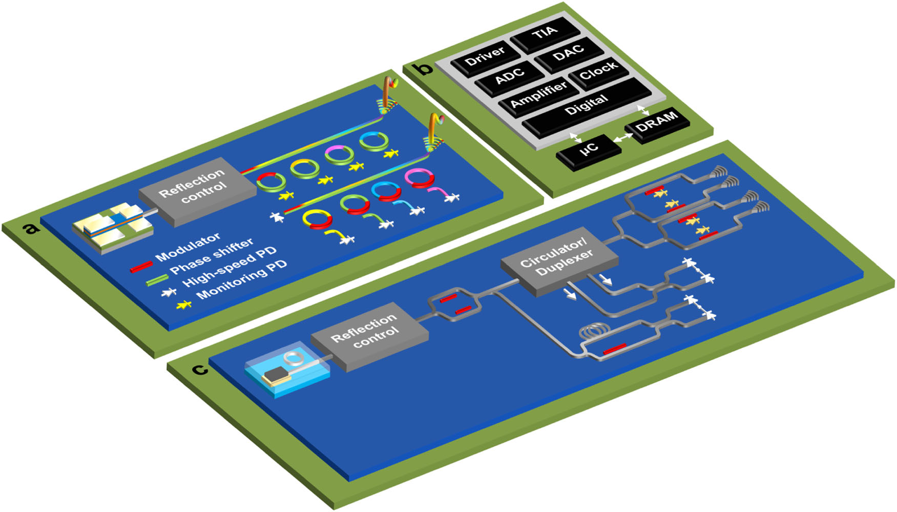
The generational roadmap Figure 1 maps the evolution of silicon photonics. Silicon-based photonic integrated circuits (PICs) were introduced in 1985 and low-loss waveguides in a thick silicon on insulator (SOI) process demonstrated in 1991–92. Various optical devices were next demonstrated6 , and soon, silicon photonics was in the small-scale integration (SSI) era— with 1-to-10 components on a PIC. They included demonstrations of high-speed pn junction modulators and photodetectors (PDs), as well as heterogeneous integration of a III-V laser to a silicon PIC. The next era ushered in the commercial success of silicon photonics. With 10-to-500 components on a PIC, this medium-scale integration (MSI) era saw successful demonstration and adoption of Mach-Zehnder modulator (MZM) in intensity-modulated direct-detect (IMDD) transceivers within data centers—both single-wavelength and multiwavelength. Microring-modulator (MRM)-based IMDD transceivers (see Fig. 2a) demonstrated the multiplexing and energy-efficiency benefits of PIC technology. Coherent transceivers in silicon photonics/electronics platforms proved that the technology could compete in performance with their LiNbO3 photonic and III-V electronic counterparts. Besides communications, silicon photonics also found new applications such as evanescent-field biosensors. Silicon photonics is now embarking on the next era of large-scale integration (LSI)—towards 500-to-10,000 components on the same chip. Applications for LSI include LIDAR (see Fig. 2b), image projection, photonic switching, photonic computing, programmable circuits, and multiplexed biosensors. Even VLSI (>10,000 components) prototypes have now been demonstrated. In the field of communication, which has been the essential market driver for silicon photonics, silicon photonics has transformed from a challenger technology in the SSI era to arguably a dominant technology in the MSI era for intra-, and inter-datacenter interconnects, and it is poised to become the incumbent technology in the LSI era. For co-packaged optics (CPO) to succeed, highperformance computing to scale22, and disaggregated computing to become a reality, silicon photonics will be pivotal.

Fig. 1 | Timeline for the number of components on a silicon photonic integrated circuit (PIC) over generations of small-scale, medium-scale, large-scale, and very-large-scale integration (SSI, MSI, LSI, VLSI, respectively).

Fig. 2 | Illustrative renditions of LSI silicon photonic systems capturing current and future technologies. a WDM Transceiver.
E/O modulation
The central quest for the next decade in shrinking photonic chips and thus increasing density is to find the elusive ‘ideal’ modulator in silicon photonics—small in length (L), requiring a small drive voltage to incur a π phase shift (Vπ), offering low propagation loss (α) and IL, and for several applications, highly linear and with large −3 dB E/O bandwidth (BW)49. Also, this modulator is preferably a phase shifter, as this enables higher-order coherent modulation formats.
Besides the topology, the PPA metrics for a modulator depend on the material and mechanism used for modulation. Table 2 shows the different materials used for modulators in various silicon photonic processes. p-n dopants utilizing the free-carrier plasma dispersion are natively available in all commercial silicon photonic foundries today, supporting 60 GHz or even higher E/O BW. Currently, the commercial market is dominated by such devices, in the form of traveling-wave MZM modulators. Plasma dispersion in Si leads to mediocre FoMefficiency, with high IL for average OMA. Carrier accumulation allows for shorter MZMs, but with BW limitations. When implemented as MRMs, the devices are much smaller, but IL and OMA remain suboptimal to support LSI/VLSI ICs.
Integration proximity of the (dissimilar) materials in direct bonding facilitates superior optical coupling and heat transportation between them. However, very smooth and clean surfaces are required. Chemical mechanical polishing (CMP) procedures, already used in high-volume manufacturing (HVM) for heterogeneous direct bonding of InP to Si for lasers, must be optimized for a scalable modulator integration pathway. Annealing is needed for strong molecular bonding and outgassing, but the pre-processed SOI wafer significantly restricts the annealing temperature. Therefore, “lowtemperature” annealing at <350℃ is usually used, but this necessitates developing custom outgassing techniques and direct bonding recipes that require extensive resources to improve yield. Mismatches in the coefficient of thermal expansion (CTE) must also be minimized. Surface topography requirements can be relaxed, and bonding strengthened using an intermediate adhesive but thermal dissipation, longterm stability, optical power handling, and drift properties need to be studied further.
Laser integration
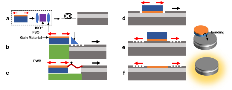
Silicon’s indirect bandgap prohibits efficient optical gain that is necessary for a laser (CW carrier) on the PIC. This deficiency requires alternative materials or methods to introduce light sources on a silicon chip, and the developments over the past decades have led to different solutions (Fig. 3). The conventional technique is to fiber-attach the PIC with a laser and an isolator (Fig. 3a). More scalable approaches integrate III-V gain materials with the PIC without fiber. But an isolator is still needed if the laser cannot tolerate reflections. Off-chip isolators perform well but are bulky and increase packaging complexity and cost. Pragmatically, it is often possible to design chips and packages in such a way that back-reflections are not a limiting factor; the high losses in the transmit path provide a barrier between the outside world and any light source. And the cost of compact isolators can be managed when designed into the package. On-chip reflection-control approaches (Fig. 2) that can eliminate the need for bulky isolators include carefully designing the photonic components to reduce reflections below the tolerance threshold of the laser, reducing the reflection sensitivity of the laser by using quantum dot gain regions with low linewidth enhancement factor, monolithic integration of magneto-optical materials (e.g., Ce:YIG), spatiotemporal modulators, or active reflection cancellation circuits. A generalized, low-cost, scalable, on-chip, low-loss, low-power, and compact solution robust to near- (coherent) and far-end (incoherent) modulated multiwavelength reflections remains a research problem.

Fig. 3 | Techniques to attach a laser to a silicon PIC. a Conventional laser-isolator (ISO)-fiber-PIC with free-space optics (FSO). b Hybrid 2.5D with FSO. c Hybrid 2.5D with photonic wire bonding (PWB). d Hybrid 3D (flip chip or transfer printing e Heterogenous (Direct bonding or transfer printing). f Monolithic (Heteroepitaxy).
A pragmatic solution for laser integration is hybrid integration, where multiple chips from different material technologies are copackaged together. For example, (sub)-mm DFB lasers, manufactured by the millions for datacom applications at low cost and high yield and pre-tested, can be co-packaged with a silicon photonic chip or even with a wafer. A 2.5D integration technology that has been commercially successful involves packaging known-good lasers with the silicon photonic die using epoxy, ball-lens, and isolator (Fig. 3b). Other 2.5D techniques include using butt coupling or photonic wire bonding to enable relaxed alignment tolerances (Fig. 3c). These 2.5D techniques are adequate for several bespoke silicon photonic applications today. Hybrid 3D integration technologies (flip-chip or micro transfer-printing) promise to further shrink the assembly size at the cost of using the PIC area (Fig. 3d), but require high-accuracy placement and bonding.
Photonics & electronics ecosystem It is insightful to look at the electronics industry ecosystem briefly. Moore’s law demonstrates that the cost per component goes down with every generation of CMOS technology reducing the critical dimensions of the transistors. This scaling is enabled by an exponential increase over time in the economic scale of the semiconductor industry, which allows the industry to pay for ever more expensive foundries and process development. Foundries enable many users to access these advanced processes, without each needing to pay to develop the process on their own. At the most extreme, the MPW (multi-project wafer) runs that the foundries host allow multiple users to share the costs of a single wafer run to develop products cost-efficiently.
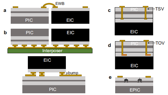
Once the chips are fabricated, there is a rich ecosystem of test houses, packaging service providers, and so forth. Electrical wirebonding (Fig. 4a) and flip-chip bonding (with C4 bumps and microbumps, Fig. 4b) are reliable and popular means of packaging, with the latter providing more bumps instead of just peripheral connections. More advanced packaging techniques (see Fig. 4) such as throughsilicon via (TSV), TSV-less interposers, and heterogeneous integration are used to improve signal integrity, power and thermal distribution, and die yield by breaking complex and large SoCs into smaller chiplets126. Because the FPGAs, GPUs, and CPUs are produced in HVM, the overall cost still goes down despite the complex packaging techniques. Nevertheless, judicious packaging decisions are made to avoid unnecessary complexity; generally, the simplest package is best, and advanced packaging techniques (chip on wafer, chip stacking, etc.) tend to be introduced only when no other alternative is feasible.

Fig. 4 | Comparing different techniques to attach a PIC to an electronic IC (EIC). a Electrical wire bonding (EWB) side-by-side. b 2.5D flip-chipped side-by-side or stacked. c Hybrid 3D TSV (Through-Silicon Via). d Heterogenous 3D with TOV (Through-Oxide Via). e Monolithic electronic photonic IC (EPIC).
Summary and conclusion
We have made big leaps in silicon photonics—from building the first high-confinement waveguides and the very first modulators only a couple of decades ago—to a technology that has strategically leveraged materials, integration and packaging techniques from the CMOS industry to become the dominant technology in the transceiver space. At the same time, silicon photonics is still very much a technology in development, and a gamut of possibilities, only some of which are described in this article, signify the prospects that lie ahead. Some clear winners will emerge in the next decade and consolidation will happen. Still, the diversity of applications will ensure ample opportunities for the technology to both scale up and spread wide.
上一篇: 碳纳米管集成电路技术的路线图和技术挑战
下一篇: 一种高效的Ge(100)表面清洁方法