Monolayer molybdenum disulfide (MoS2), an emergent two-dimensional (2D) semiconductor, holds great promise for transcending the fundamental limits of silicon electronics and continue the downscaling of field-effect transistors. To realize its full potential and high-end applications, controlled synthesis of wafer-scale monolayer MoS2 single crystals on general commercial substrates is highly desired yet challenging. Here, we demonstrate the successful epitaxial growth of 2-inch single-crystal MoS2 monolayers on industry-compatible substrates of c-plane sapphire by engineering the formation of a specific interfacial reconstructed layer through the S/MoO3 precursor ratio control. The unidirectional alignment and seamless stitching of MoS2 domains across the entire wafer are demonstrated through cross-dimensional characterizations ranging from atomic- to centimeter-scale. The epitaxial monolayer MoS2 single crystal shows good wafer-scale uniformity and state-of-the-art quality, as evidenced from the ~100% phonon circular dichroism, exciton valley polarization of ~70%, room-temperature mobility of ~140 cm2 v−1 s−1 , and on/off ratio of ~109 . Our work provides a simple strategy to produce wafer-scale single-crystal 2D semiconductors on commercial insulator substrates, paving the way towards the further extension of Moore’s law and industrial applications of 2D electronic circuits.
Since the creation of integrated circuits in the 1960s, silicon transistors, following the Moore’s law, have been shrinking to boost performance and reduce costs over the past half a century. Today, as conventional silicon transistors enter the sub-10 nm technology node and approach their physical limits, new channel materials are urgently required to further scale transistors and extend Moore’s law beyond silicon electronics. Two-dimensional (2D) semiconductors with atomic thicknesses and dangling-bond-free flat surface have attracted tremendous interest and possess promising prospects for scaling transistors to the end of roadmap. The International Roadmap for Devices and Systems (IRDS) has listed 2D semiconductors as the potential channel materials in 2017, and forecasts that 2D electronic circuits will be commercially available by 2034.
Monolayer molybdenum disulfide (MoS2) has been considered as one of the most promising 2D semiconductor candidates for high performance electronic circuits because of its intrinsic high mobility, excellent gate controllability, high on/off current ratio, ultra-low standby current, small dielectric constant, and good stability. Indeed, isolated monolayer MoS2 devices have been successfully demonstrated to perform well at ultra-scaled lengths down sub-1 nm, which are inconceivable in the framework of traditional silicon with scaling gate length limit of ~12 nm. Monolayer MoS2 transistors have also been identified by Intel as one of three breakthrough technologies to break the scaling limit of silicon. To realize its full potential and high-end industrial applications, it is of utmost importance and a prerequisite to product wafer-scale monolayer MoS2 single crystals on commercial substrates.
Results
Unidirectional domain alignment by buffer layer control
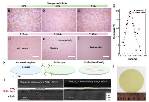
Figure 1a–c presents the optical micrographs of the as-grown MoS2 triangular domains on c-plane sapphire substrates with a major miscut angle (~0.2°) towards M-axis under three representative MoO3/S precursor ratios: 3.9% (Fig. 1a), 4.5% (Fig. 1b) and 5.1% (Fig. 1c). Remarkably, the degree of unidirectional alignment strongly depends on the MoO3/ S precursor ratio.

Fig. 1 Unidirectional domain alignment enabled by buffer layer control.
Seamless stitching of MoS2 domains To realize the goal of wafer-scale single-crystal MoS2 monolayers, seamless stitching of aligned grains must also be satisfied simultaneously, in addition to the unidirectional domain alignment. To verify the seamless stitching and the absence of grain boundaries, partially merged MoS2 domains were characterized by atomicresolution aberration-corrected HAADF-STEM. Figure 2a shows a low-magnification STEM image from the merged area of the two aligned MoS2 domains. The angle between two merged MoS2 grains is ~60°. Figure 2b displays six representative atomic-resolution STEM images taken at the corresponding locations marked in Fig. 2a. The identical lattice orientation without grain boundary continuously across the merging zone strongly evidences the seamless stitching of the MoS2 domains and therefore single-crystal nature. Additionally, the atomic-resolution STEM images show a honeycomb lattice with d-spacing of 0.158 nm and 0.274 nm, corresponding to the (1120) and (1010) planes of monolayer MoS2, consistent with previous work43. More STEM images of merged areas that support the seamless stitching of MoS2 domains can be found in Supplementary Note 10.

Fig. 2 Seamless stitching of unidirectional MoS2 domains.
Polarized second-harmonic generation (SHG), which is highly sensitive to grain boundaries44,45, is further performed to confirm the seamless stitching of MoS2 domains at the large scale. Figure 2c shows the representative polarized SHG mapping of two unidirectionally merged domains. Uniform signal is observed with no obvious intensity fluctuations across the merging area. This is strongly distinct to the antiparallel domains, where a dark line appears at the grain boundary (Fig. 2e). Figure 2d presents the polarized SHG mapping of a continuous MoS2 film consisting of unidirectional aligned domains, showing a uniform distribution of intensity over the entire area. This provides a strong proof of the absence of grain boundaries and seamless stitching, in contrast to result of polycrystalline MoS2 film (Fig. 2f). Besides, etching experiments with hot water vapors are also performed to verify the seamless stitching of unidirectional aligned MoS2 domains (Supplementary Note 11).
Wafer-scale uniformity and high quality
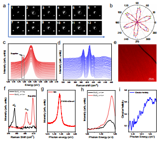
The quality and uniformity of the as-grown single crystal monolayer MoS2 wafers are illustrated via multi-scale characterizations. Figure 3a presents the low-energy electron diffraction (LEED) patterns measured at twelve random locations across over an area of more than 1 cm2 . The essentially identical LEED patterns provide strong evidences of the uniformity of the as-grown single crystal monolayer MoS2. In addition, the LEED patterns show three bright diffraction spots, which unambiguously proves the three-fold rotational symmetry and therefore the single-crystalline nature of the as-grown monolayer MoS2 film (Supplementary Note 12)21. Figure 3b is the stacked nine polarizationresolved SHG patterns across a 1 cm2 sample area (SHG patterns from different locations are indicated by different colors). The nearly overlapped SHG six-petal patterns confirm the coherent lattice orientation and uniformity of the as-grown monolayer MoS2 film. Figure 3c, d shows 25 representative room-temperature Raman and photoluminescence (PL) spectra across a 2-inch MoS2 wafer, respectively (please also refer to Raman and PL mapping in Supplementary Note 13). No apparent changes in the peak position and linewidth of both phonons and excitons are observed, illustrating the wafer-scale uniformity. Figure 3e presents a representative fluorescence microscope image of the as-grown monolayer MoS2. The uniform color contrast confirms the uniformity of the monolayer MoS2 film. The wafer-scale uniformity of the as-grown monolayer MoS2 single crystal is also scrutinized by optical micrographs taken at different locations across a 2-inch range (Supplementary Note 14).

Fig. 3 | Wafer-scale uniformity and high quality.
Discussion
In conclusion, we demonstrate a simple strategy of precursor ratio control for the batch production of wafer-scale single-crystal MoS2 monolayer films on industry-compatible substrates of c-plane sapphire. The epitaxial monolayer MoS2 single crystals exhibit wafer-scale uniformity and the state-of-the-art properties, evidenced by the perfect phonon circular dichroism, exciton valley polarization of ~70%, room-temperature mobility of ~140 cm2 v−1 s−1 , on-current density of ~535 μA/μm, and a nearly 109 on/off ratio. Our work offers a novel insight into the synthesis of wafer-scale high-quality 2D semiconductors and lays a solid foundation for industrial applications of 2D integrated electronic circuits.
上一篇: 电子级多晶硅从硅芯到表面的微观结构演变
下一篇: 微流控器件制造的双铸造方法比较