Abstract: Large-size electronic-grade polycrystalline silicon is an important material in the semiconductor industry with broad application prospects. However, electronic-grade polycrystalline silicon has extremely high requirements for production technology and currently faces challenges such as carbon impurity breakdown, microstructure and composition non-uniformity, and a lack of methods for preparing large-size mirror-like polycrystalline silicon samples. The article innovatively uses physical methods such as wire cutting, mechanical grinding, and ion thinning polishing to prepare large-size polycrystalline silicon samples that are clean, smooth, free from wear, and have clear crystal defects. The material was characterized at both macroscopic and microscopic levels using metallographic microscopy, scanning electron microscopy (SEM) with backscattered electron diffraction (EBSD) techniques, and scanning transmission electron microscopy (STEM). The crystal structure changes from single crystal silicon core to the surface of the bulk in the large-size polycrystalline silicon samples were revealed, providing technical basis for optimizing and improving production processes.
1. Introduction
Polycrystalline silicon, as the basic material for the electronics and photovoltaic industries, is widely used in fields such as artificial intelligence, automatic control, information processing, and solar power generation. It is known as the "cornerstone of microelectronics." Due to the growth in the photovoltaic and integrated circuit industries, the apparent demand for polycrystalline silicon in China has been continuously increasing in recent years. Polycrystalline silicon can be classified into two categories based on purity: solar grade (6N-9N) and electronic-grade (9N-11N). Electronicgrade polycrystalline silicon is one of the purest substances obtained in human industry. Currently, there is a significant gap in the supply of electronic-grade polycrystalline silicon.
However, the production of electronic-grade polycrystalline silicon requires extremely high technical standards and faces the following challenges. Carbon is a major impurity in semiconductor materials that can significantly impact electrical performance, particularly in silicon devices. It can induce breakdown voltage and pose a risk to high-power thyristor devices. High concentrations of carbon in polycrystalline silicon promote the formation of oxygen precipitates. the combined effects of carbon and oxygen complicate the influence of impurities on material and device performance, resulting in shortened lifespan. Additionally, the non-uniform microstructure and composition of polycrystalline silicon can greatly affect its quality stability. These issues are influenced by process parameters and techniques during production. These two challenges greatly hinder the large-scale production of electronic-grade polycrystalline silicon with a diameter of 12 inches or above. The technical bottlenecks in the electronic-grade polycrystalline silicon industry may further impact downstream semiconductor companies and chip manufacturing.
2. Sample preparation and characterization methods
2.1. Metallographic sample preparation
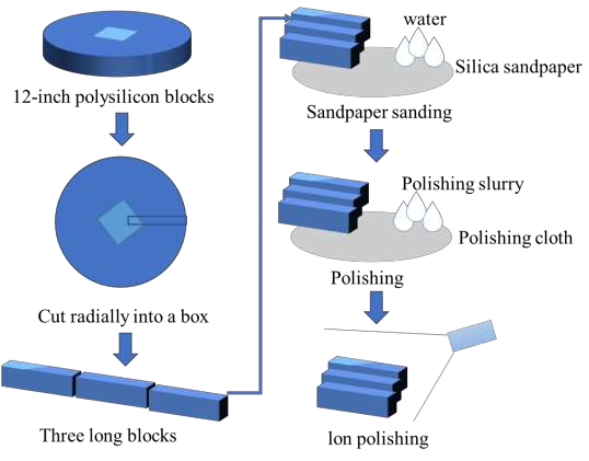
As shown in Figure 1, the large 12-inch polycrystalline silicon block(The silicon core size is 30 mm × 30mm) is cut into three long strip-shaped blocks measuring 20 mm × 5 mm × 5 mm from the core towards the outer side using wire cutting, and their orientations are marked. Manual grinding is performed on a rotating disc using silicon dioxide paper with sequentially decreasing particle sizes of 800 to 4000 grit. During the grinding process, it is important to apply balanced force until the scratches appear neat and uniform under an optical microscope. Finally, polishing is performed using silicon dioxide polishing suspension (0.05 μm) to achieve a matte finish. Subsequently, the sample is thoroughly cleaned by ultrasonication in anhydrous ethanol and acetone to remove any residual hydrocarbons on the polished surface.

Figure 1. Schematic diagram showing metallographic sample preparation of 8-inch polycrystalline silicon rod.
2.2. Material characterization methods
To investigate the morphological, dimensional, and orientational variations of the grains in different regions of large polycrystalline silicon blocks, we initially employed an optical microscope to observe the structural changes from the silicon core to the outer surface of the polished samples. Subsequently, we conducted microscopic observation and orientation characterization of the material using a scanning electron microscope (SEM) equipped with electron backscatter diffraction (EBSD) and a scanning transmission electron microscopy (STEM).
Electron backscatter diffraction (EBSD) is a technique that utilizes diffracted electron beams to obtain crystallographic information about the sample. By analyzing the orientation structure information carried by the backscattered electrons, we can acquire comprehensive insights into grain boundaries, phases, grain orientations, textures, and strains within the sample. Focused Ion Beam (FIB) is a technology that utilizes ion beams for processing and analysis. It is based on controlling the energy and focus of the ion beam and can precisely etch, cut, deposit or implant the material. FIB typically uses high-energy ion beams, such as argon ions or radium ions, which are focused to very small diameters by a focusing device, allowing for high-resolution processing and analysis. The focused ion beam has the advantages of high precision, high resolution and non-contact. Focused ion beams are widely used in various fields. In the semiconductor industry, it is used for tasks such as chip repair, circuit modification, and sample preparation. In the field of materials science and nanotechnology, FIB can be used to prepare nanodevices, etch nanostructures, and characterize samples. In this paper, high quality samples for TEM characterization were obtained by fib. Scanning transmission electron microscopy is a technique used in the field of electron microscopy to study the structure and composition of materials at the atomic scale. In this paper, the required data was obtained by using the FIB of Thermo Scientific Helios 5 ux equipped with EBSD, with an electron beam operating voltage of 5 kV and an ion beam operating voltage of 30 kV. In STEM, a focused electron beam is scanned across the sample, and the transmitted electrons are collected and used to form an image. This allows for high-resolution imaging of the sample, providing valuable information about its structure and properties. In this paper, the required data was obtained by using STEM model JEM-ARM300F2 with an operating voltage of 300 kV.
3. Results & Discussion
3.1. Metallurgical microscope characterization from core to surface of polycrystalline silicon
3.1.1. Silicon core
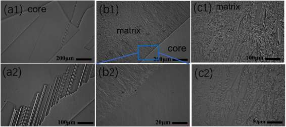
Figures 2(a1, a2) reveals the characteristics of the microstructure of the silicon core. Overall, the silicon core exhibits a typical single-crystal structure, with a smooth and even surface, and no presence of minor dendrites. The interior of the single-crystal silicon core displays abundant subgrain structures. In Figures 2(a1, a2), we can clearly observe blocky subgrains, mostly in square or rectangular shapes, with smooth and neat edges, relatively clean interiors, and a low defect rate. Further observation in Figures 2(b1, b2) reveals interconnected elongated twins with consistent orientation, with grain widths ranging from 30 μm to 100 μm and exhibiting smooth and sharp boundaries.

Figure 2. Metallographic micrograph of a polycrystalline silicon matrix: (a1-a2) the core of polycrystalline silicon; (b1-b2) the interface of polycrystalline silicon; (c1-c2) the matrix of polycrystalline silicon.
3.1 Interface between the core and matrix
As shown in Figure 2(b), a clear interface is evident between the silicon core and the matrix of the material, with an amorphous region at the interface. The emergence of the amorphous region is attributed to the discontinuity between different crystal structures and the mismatch in atomic arrangements. At the interface between single-crystal and polycrystalline regions, atomic diffusion may occur under the influence of temperature or stress. Such diffusion can lead to structural disorder and the formation of amorphous regions. The presence of amorphous interfaces typically introduces electron scattering, restricts carrier mobility, leads to electron-hole recombination, and subsequently affects carrier lifetime, ultimately resulting in decreased conductivity. The presence of amorphous interfaces also affects the band structure of polycrystalline silicon, potentially leading to the formation of additional charge states near the interface, consequently influencing electron band filling and migration.
3.2. SEM-EBSD characterization from core to surface of polycrystalline silicon
3.2.1. Silicon core
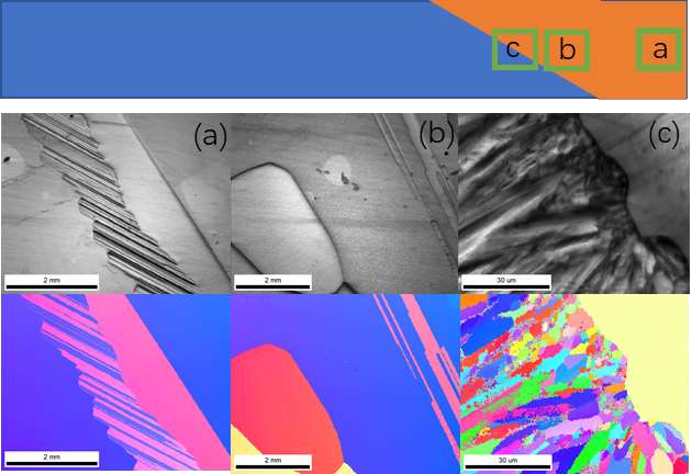
As depicted in Figures 3(a, b), the SEM and EBSD images illustrate the internal structure of the large polycrystalline silicon core. Throughout this process, we observe an increase in the number and length of elongated, strip-shaped features from the core to the edge region, gradually coalescing into large subgrains. The edge region predominantly exhibits large subgrains, with a higher abundance. The boundaries of the large subgrains are characterized by a multitude of stacking faults and dislocation defects, the accumulation of which results in structural non-uniformity at the boundaries. Furthermore, the junctions of multiple subgrains can lead to issues of stress concentration .

Figure 3. SEM-EBSD plot of the polysilicon: (a, b) Abundant twins and subgrains in silicon core; (c) interface between the singlecrystal core and polycrystalline matrix within the large-sized polycrystalline silicon.
3.2.3. Matrix
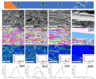
As depicted in Figure 4, the SEM and EBSD images vividly illustrate the evolution of the internal structure of polycrystalline silicon, gradually moving away from the silicon core, from region a to region d. In Figure 4(a1-4), the vicinity of the interface exhibits the gradual reduction and termination of large columnar grain crystals, forming a divergent, chrysanthemum-like grain morphology. The grain sizes primarily range between 20 μm and 60 μm, exhibiting low-angle specific orientation. Notably, there are numerous micrometer-sized small grains present in the interstices between the grains, serving as a cushion to mitigate stress concentration issues when different-oriented large grain crystals come into contact. Overall, the matrix near the single crystal core predominantly exhibits a chrysanthemum-like grain structure, with micrometer-sized small grains filling the gaps.

Figure 4. SEM-EBSD plot at the boundary of the polysilicon matrix: (a1-a2) Columnar grain crystals and chrysanthemum-like grain morphology at the vicinity of the interface; (b1-b2) Small grains with random orientation and grains with certain orientations in the midsection of the polycrystalline region; (c1-c2) Columnar crystal structure in the tail end of the polycrystalline region; (d1-d2) Twins in edge of the polycrystalline region.
4. Conclusions
The large-scale electronic-grade polycrystalline silicon is an important material in the semiconductor industry with promising prospects. With the rapid development of information technology, the demand for semiconductor products continues to increase, and electronic-grade polycrystalline silicon, as a crucial component of semiconductor materials, will continue to be in high demand. The innovative use of physical methods such as wire cutting, mechanical grinding, and ion thinning polishing in the preparation of large-sized polycrystalline silicon samples with clean, smooth surfaces, no wear, and clear crystal defects is documented in this paper. The material was characterized from macroscopic to microscopic levels using metallographic microscopy, electron backscatter diffraction and scanning electron microscopy technique. We have used advanced characterization techniques, such as STEM, for more detailed microscopic structural details.
上一篇: 半导体封装过程中晶圆缓冲区缺陷检测