Abstract
Efectively detecting defects in wafer bufer zones is crucial in semiconductor manufacturing processes. If defects are not detected in the middle of the semiconductor manufacturing process, the semiconductor eventually becomes a defective product after all processes are completed. To solve this problem, rule-based vision algorithms have been used to identify defects in the wafer bufer zone. After photographing the wafer bufer zone using a high-speed camera, defects are detected using the pixel values of the images. However, because of the resin bleed in the wafer, which is an epoxy compound, it is difcult to detect defects. Therefore, we introduced a deep learning method for semiconductor inspection and created a high-performance semiconductor inspection algorithm. The defects in the wafer bufer zone should be detected accurately and quickly. Furthermore, the approximate size of the defects must be extracted. We modifed the Xception model to ft the wafer data characteristics considering both accuracy and speed. We proposed to extract the size of the defect using class activation mapping (CAM). We obtained an accuracy of 96.9% from the actual wafer dataset through this framework, and then managed to extract the size of the defect through CAM.
Introduction
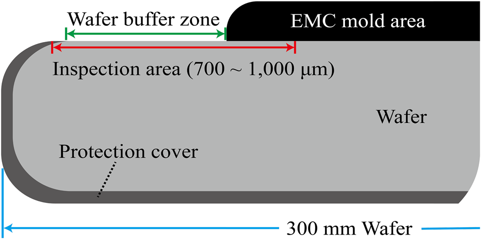
Semiconductor wafers undergo various packaging processes and unwanted defects must be accurately and quickly detected during each process. However, epoxy molding compounds (EMC) used to protect semiconductor devices from external impact, vibration, moisture, and radiation as well as the protection cover in the bottom of wafers make the visual and in-process detection of defects difcult (Fig. 1). While defects in wafers can be checked after all processes are completed, the manufacturing loss due to reduced yield becomes non-negligible. Fortunately, there is a narrow region not covered with EMC mold called the wafer bufer zone which can be observed during the process. Hence, real-time inspection of this zone for detecting wafer defects during the process is important.

Fig. 1 Schematic representation of inspection area
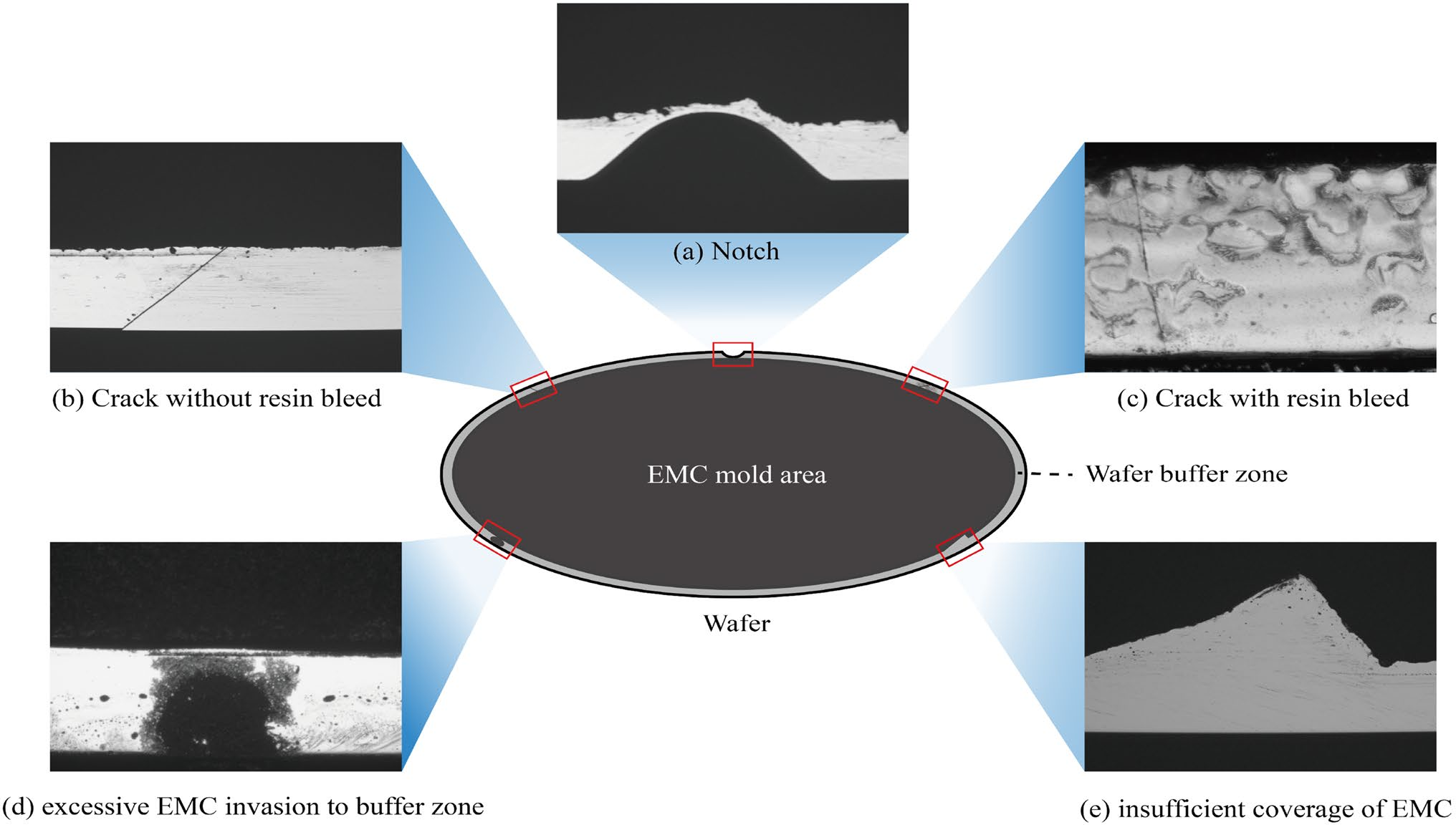
Images obtained from the inspection of the wafer bufer zone can be classifed into four types: Normal, Crack, EMC defect, and Notch (Fig. 2). Notch (Fig. 2a) is the reference point of the wafer and hence is not a defect. We would like to detect cracks and EMC defects when inspecting the wafer bufer zone during the packaging processes. It is relatively easy to detect cracks when they exist on a clean surface (Fig. 2b). However, the detection becomes difcult when cracks appear on a surface with resin bleeding (Fig. 2c), especially if they are relatively small. EMC defects occur when they are not properly cover the mold area where the semiconductor die is located (Fig. 2d, e). If EMC excessively invades the bufer zone, the protecting cover can stick to it and cause damages to the wafer. If EMC in the mold area is insufcient, the semiconductor die cannot be fully protected. These EMC defects are not easy to be detected as they can be confused with notch or resin bleeding, which is normal.

Fig. 2 Types of images obtained during inspection
For the detection of these wafer defect, rule-based computer vision algorithms can be used. For example, the Sobel operator can be used to detect edges of images and identify defects. However, it is difcult to extract cracks using this operator if the wafer bufer zone is covered with resin bleeding because too many edges are extracted. Another popular approach is the Canny algorithm which extracts the meaningful edges by thresholding after denoising images using Gaussian flters. While this algorithm generally provides better results than the Sobel operator, it sufers from the same difculty in distinguishing cracks from resin bleeding.
Recently, various deep learning models that use high level features have been developed in computer vision. For example, object detection models recognize an object from an image by indicating its location in a bounding box. Semantic segmentation models classify objects more densely than the detection model using the pixels within an image. While we can know the location and size of defects with these models, they require bounding-box annotations or segmented labels for training. Also, these models are heavy in terms of the number of model parameters and require a long time for training and inference. Since the detection of wafer defects needs to be done quickly during the packaging processes, these models cannot be used directly in practice.
Alternatively, we can use the classifcation model which classifes images into the defned types. It is lighter than detection and semantic segmentation models, and hence, is advantageous in terms of speed. In addition, there is no need to annotate labels in images when building the datasets for training. However, this model is unable to localize the defects within an image and measure their characteristic features such as the size and the area.
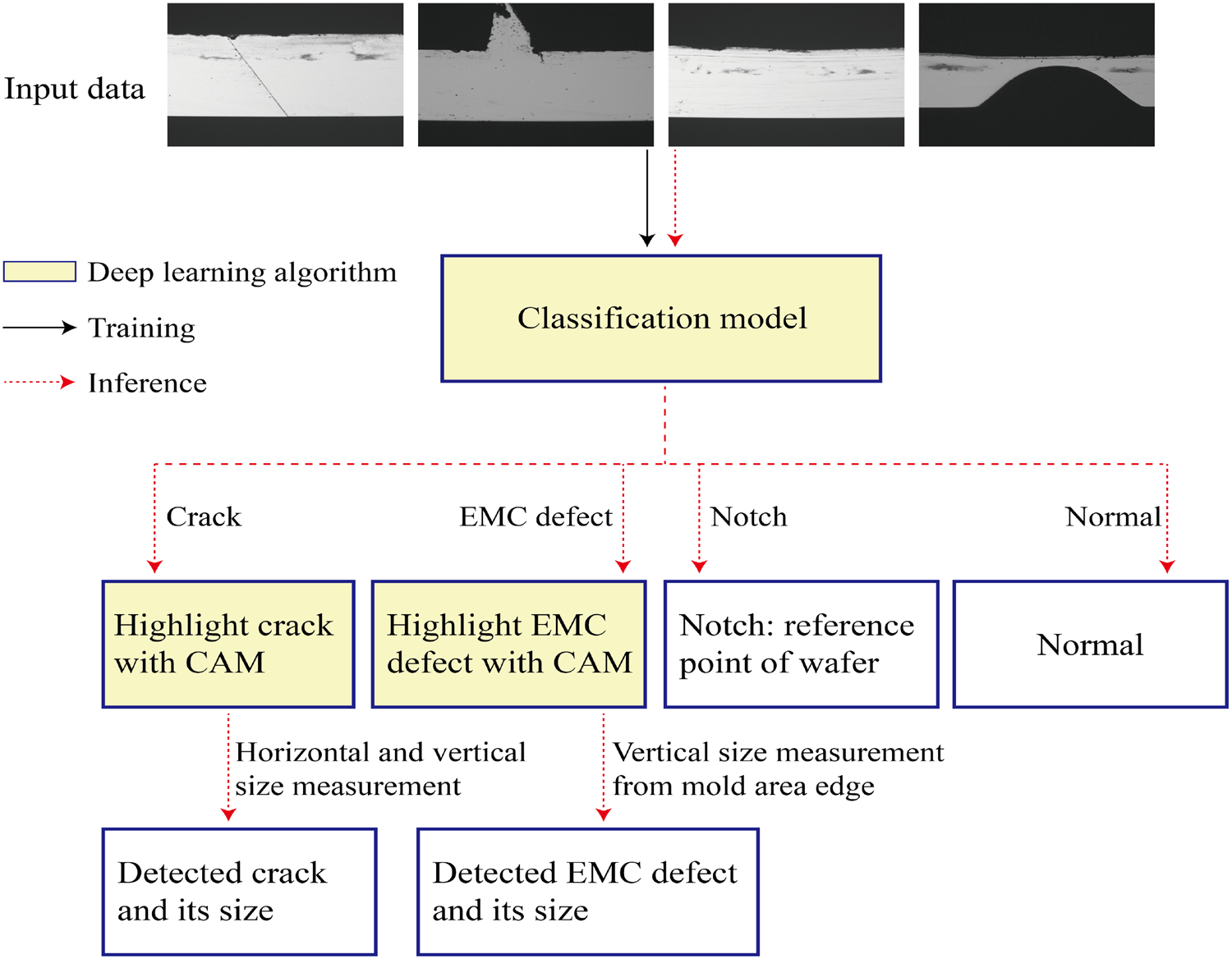
In this study, we develop a deep learning-based inspection method for detecting defects in the wafer bufer zone. The model was designed to fnd and localize a defect quickly, and infer its size as well (Fig. 3). We employed a classifcation model, Xception, and modifed it to be suitable for inspecting the wafer bufer zone. To accelerate the inspection, we changed eight repetitions of middle fow of the original Xception model to one. In addition, the feature pyramid network (FPN) was used to efectively handle various sizes of defects. We utilized the class activation map (CAM) to generate a heat map of a specifc class image, and hence, estimate the size of defects without any additional supervised learning. The length of cracks and the area of EMC defects can be approximately obtained while inspecting the wafer bufer zone. The proposed model showed higher detection accuracy and faster inference speed than baseline models.

Fig. 3 Overall workfow. The training fow and inference fow are represented with black solid lines and red dashed lines, respectively
Inspection model consists of the image classifcation for identifying defects and the estimation of their size (Fig. 4). The Xception deep learning model was employed for classifcation with modifcation to enhance the efciency in detecting defects. The class imbalance problem was alleviated by adopting the focal loss. The identifed region of defects in the wafer bufer zone was inspected with CAM to estimate the size of cracks and EMC defects.
上一篇: 通过优化阴影蒸发技术改善晶圆尺度均匀性
下一篇: 电子级多晶硅从硅芯到表面的微观结构演变