One of the practical limitations of solid-state quantum computer manufacturing is the low reproducibility of the superconducting qubits resonance frequency. It makes hard demands on the Josephson junction fabrication process, producing a nonlinear inductance of the qubit. In this work, we demonstrate for 100 mm wafer diameter decreasing of the room temperature resistance variation coefficient 𝐶𝑉𝑅𝑁 to 6.0% for 0.025 μm2 Al/AlOx/Al Josephson junction area and to 4.0% for 0.090 μm2 Al/AlOx/Al Josephson junction area. These results were achieved by the development of the shadow evaporation process model considering the Josephson junction area variation on the wafer. Our model allows to provide of the junction area variation coefficient 𝐶𝑉𝐴 about 1.0% for Josephson junctions characteristic dimensions from 100 nm to 700 nm. In addition, we show of the junction oxidation technic optimization. Our improvements can be scalable on the wafer with a large diameter, which allows to manufacturing of the quantum processor with high reproducibility of electrical parameters.
In the last years, one of the most priority challenges is solid-state quantum computer manufacturing, which helps to exponentially increase the calculation power for practically useful tasks solving. There are several perspective platforms for quantum computer building as trapped ions, semiconductor quantum dots, NV center in diamonds and superconducting quantum bits. Quantum circuits based on superconducting artificial atoms (Josephson junctions) are distinguished by good scalability and control. Only for the last few years superconducting 54-qubits quantum processor Sycamore (Google company), 127-qubit processor Eagle and -qubit processor Condor (IBM company) and others were demonstrate. However, the main limitation of the scalability of quantum processors based on the fixed-frequency transmon qubits is a requirement to the detuning of the resonance frequency between them. For example, the cross-resonance gate architecture requires less than 6 MHz standard deviation of qubit frequencies in order to scale beyond 1000 qubits . Collisions of the resonance frequency contribute to increasing the quantum gate time and other negative factors decreasing the fidelity. Another device demanding the high reproducibility of the Josephson junction’s parameters is Josephson Travelling Wave Parametric amplifier (JTWPA). This device consists of several hundred identical elementary cells each of them are LC-C oscillator involved in the parametric amplification process. JTWPA provides an exponentially increasing gain if the reproducibility of elementary cells electrical parameters larger than 98%.
Fabrication and resistance characterization
For Josephson junctions forming we used the standard Dolan bridge technique. In our previous works we show that the Dolan bridge method needs a smaller evaporation angle compared with Manhattan style technique that helps to provide less electrode edge roughness. In this study, we used a two-layer organic mask formed by the spin-coated method, where bottom layer is 500 nm MMA-EL9 copolymer and top layer is 100 nm AR-P 6200 (CSAR) resist. The topology was exposed by 50 keV electron-beam lithography tool. The exposure dose needed for the development of small elements is 160 μCl/cm2 . We used a beam step value of less than 5 nm and a beam current of 0.4 nA for high reproducibility of linear dimensions in organic mask and small edge roughness. We fixed a location of JJ in the center of the write field that decreased the distortion of the primary beam. We used the standard development recipe in Amylacetate for the top layer of the organic mask and IPA:DiW solution for the copolymer. Before the shadow evaporation step, the descum operation is carried out to clean the substrate from organic residues. Al/AlOx/Al electrodes are e-beam shadow-evaporated in an ultra-high vacuum deposition system. The 25 nm bottom junction electrode is oxidized at different modes to form the tunnel barrier and next the 45 nm thick top electrode is evaporated followed by a 10 min termination oxidation. The deposition rate was chosen to provide a minimum for both the root mean square surface (RMS) roughness and the line edge roughness (LER) of the bottom electrode. Since decreasing the deposition angle contributes to the minimization of RMS surface roughness of the electrode (the shading effect becomes more significant as the deposition angle increases), we used a small deposition angle 40° for the bottom electrode. We then pattern and evaporate aluminum bandages with an in-situ Ar ion milling to provide good electrical contact of the junction with the base layer. Lift-off is performed in a bath of N-methyl-2-pyrrolidone with sonication at 80°C and rinsed in a bath of IPA with ultrasonication.
Figure 1a shows the general view of the test topology. The test topology consists of 96 matrices with JJ of the three different areas as 𝐴 = 0.010 μm2 , 𝐴 = 0.025 μm2 , and 𝐴 = 0.090 μm2 . We formed 216 JJ for each area. The surface quality and the junction dimensions were measured by scanning electron microscopy.

Figure 1. (a) General view of the 100 mm wafer. The topology contains 12 chips placed at 49 cm2 working plane. Each test structure is a combination of the Josephson junction, bandage structure and Al contact pad. (b) The shadow evaporation process scheme. We used standard Dolan bridge technique for JJ forming. 𝑎1 = 40° and 𝑎2 = 0° are the evaporation angles using in this work. (c) JJ fabrication process main operations. I Al base layer evaporation, II ground layer dry etching, III electron-beam lithography of the JJ, IV bandage-structure forming. (d) Scanning electron micrographs of the Josephson junction. We formed JJ of three different areas as 𝐴 = 0.010 μm2 , 𝐴 = 0.025 μm2 and 𝐴 = 0.090 μm2 in this paper.
Measurement and results
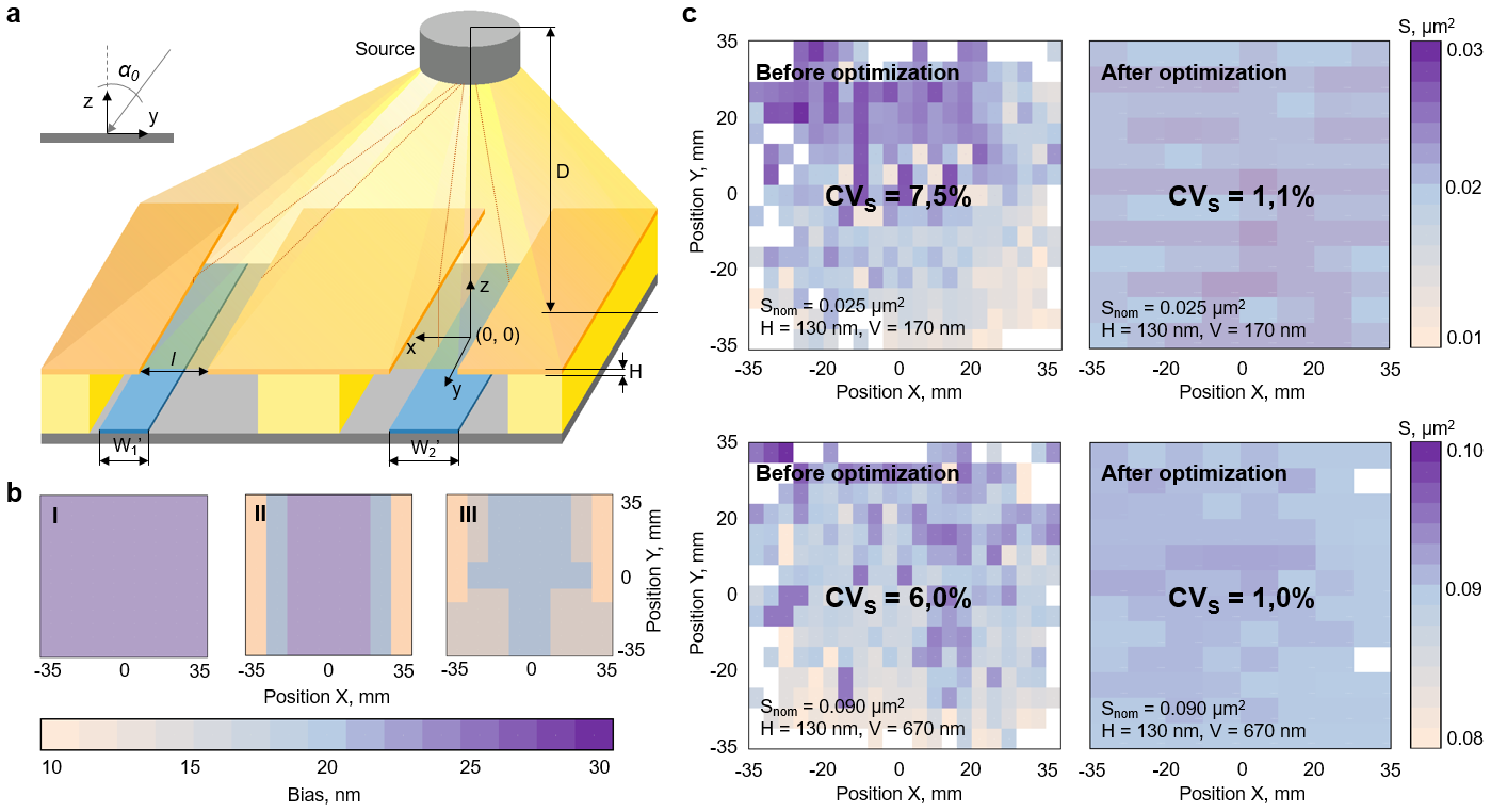
The previous researches highlights that the reproducibility limitation of 1f parameters is provided by not onlyelectron beam lithography operation but also the shadow evaporation one. this is explained a diverging metal flouforming at the electron-beam evaporation process. The conical shape of the metal flow leads to a change of theevaporation angle along the wafer and consequently to a change in the Jl characteristic dimensions. This efect is fulldescription in Ref. . We developed the shadow evaporation process model for eliminating the 1f geometry spacedependence. The model key parameters are the thickness of the top (H) and bottom (h) layers ofthe organic mask.

Figure 2. (a) The shadow evaporation model geometric representation. We show the junction dimensions changing depending on the location of the wafer. Our model takes into account the source distance 𝐷, resist thickness 𝐻, and shadow evaporation regime parameters 𝑎 . We used the non-point source model to increase the bias calculation precision. (b) Comparing the bias values depending on the shadow evaporation model representation. I Bias values excluding model parameters, II the shadow evaporation model with point source, III the shadow evaporation model with the non-point source. (c) Wafer-scale Josephson junction square-maps before and after the shadow evaporation model included. The developed model allows to decrease of the JJ area coefficient variation to 𝐶𝑉𝐴=1.0% for 0.025 μm2 and 0.090 μm2 JJ areas.
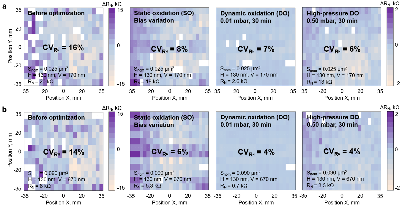
Figure 3 shows that without the shadow evaporation model, the minimum value of the room temperature resistance variation coefficient is 𝐶𝑉𝑅𝑁 = 16% for 0.025 μm2 area and 𝐶𝑉𝑅𝑁 = 14% for 0.090 μm2 area. The conical shape of the metal flow has limited the reproducibility of JJ dimensions. Our model allows a significant decreasing the variation coefficient to 𝐶𝑉𝑅𝑁 = 8% for 0.025 μm2 area and 𝐶𝑉𝑅𝑁 = 6% for 0.090 μm2 area without a change of oxidation technique (static oxidation, 4 mbar). The low-pressure dynamic oxidation technique leads to a decrease 𝐶𝑉𝑅𝑁 to 4.2%. This improvement is explained by dynamic oxidation physics when the system implements continuous supply and pumping of oxygen that provides constant updating of the reagent (O2). The oxygen has faster and more evenly diffusion at the wafer surface in these conditions which leads to the growth of the quality and homogeneous tunnel barrier [28]. We used longer oxidation time and higher oxygen pressure to obtain a thicker tunnel barrier that decreased the influence of the barrier thickness variation on JJ electrical characteristics. Increasing the oxidation pressure to 0.5 mbar and holding time to 30 minutes allows decreasing the 𝐶𝑉𝑅𝑁 value to 4% at the wafer working area. A detailed description of our experiments is given in the table 1.

Figure 3. The wafer-scale JJ room temperature resistance-map depending on the optimization step for 0.025 μm2 (a) and 0.090 μm2 (b) junction areas. Our improvements allow to decrease the room temperature resistance coefficient variation from 𝐶𝑉𝑅𝑁 = 16% to 𝐶𝑉𝑅𝑁 = 6% for 0.025 μm2 Josephson junction area and from 𝐶𝑉𝑅𝑁 = 14% to 𝐶𝑉𝑅𝑁 = 4% for 0.090 μm2 Josephson junction area.
Conclusion
In this Letter, we demonstrate the decrease ofthe room temperature resistance variation coeficient for 100 mm waferWe show CVa= 6% for 0.025 um2 Al/AlO/Al Josephson junction area and CV= 4% for 0.090 μm2 A//AIOJAIJosephson junction area by the shadow evaporation model development and the oxidation step optimization. "Theworking plane in our experiments is 70x70 mm. For 25x25 mm chip the CV = 2% for diferent areas. Based on thesimulation results we show that the highest JJ parameters reproducibility achieved with a small evaporation angle(before 45°) and small thickness of the top layer of the organic mask. We assume that the next steps to CV decreasingare optimization of' the inter face between JJ metal and substrate and post-fabrication treatment.
上一篇: 通过界面钝化开发碳_硅异质结太阳能电池
下一篇: 半导体封装过程中晶圆缓冲区缺陷检测