Passivating contactsin heterojunction (HJ) solar cells have shown great potential in reducing recombination losses, and thereby achieving high power conversion efficiencies in photovoltaic devices. In this direction, carbon nanomaterials have emerged as a promising option for carbon/silicon (C/Si) HJsolar cells due to their tunable band structure, wide spectral absorption, high carrier mobility, and properties such as multiple exciton generation. However, the current limitations in efficiency and active area have hindered the industrialization of these devices. In this review, they examine the progress made in overcoming these constraints and discuss the prospect of achieving high power conversion efficiency (PCE) C/Si HJ devices. A C/Si HJ solar cell is also designed by introducing an innovative interface passivation strategy to further boost the PCE and accelerate the large area preparationof C/Si devices. The physical principle, device design scheme, and performanceoptimization approaches of this passivated C/Si HJ cells are discussed. Additionally, they outline potential future pathways and directions for C/Si HJ devices, including a reduction in their cost to manufacture and their incorporation intotandem solar cells. As such, this review aims to facilitate a deeperunderstanding of C/Si HJ solar cells and provide guidance for their further development.
1. Background
Solar energy is considered one of the most promising renewable energy sources to reduce the consumption of fossil fuels and achieve carbon neutrality. Solar cell devices, including crystalline silicon (c-Si) solar cells, copper indium gallium selenium (CIGS), cadmium telluride (CdTe),organic solar cells and perovskite solar cells, have advanced rapidly and are striving to meet the increasing demand for clean energy. Owing to their high power conversion efficiency (PCE), long stability, and scalable mass production techniques, Si solar cells occupy more than 95% of the worldwide photovoltaic (PV) market.
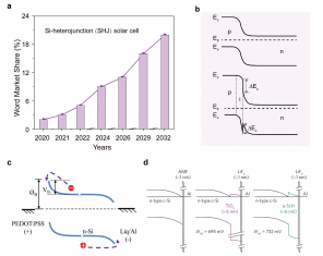
The PV effect at a p-n junction is at the heart of c-Si solar cells. A p-n homojunction is formed by diffusing a p (or n) emitter onto a n (or p) Si substrate. The aluminum back surface field (Al-BSF) cell, in which the entire rear silicon surface is alloyed with aluminum to form the device’s positive terminal, is one such solar cell that has dominated large-scale industrial PV device production for the last 30 years. This is due to its simple design and low-cost to manufacture. However, recombination losses and a high series resistance caused by metal-semiconductor interfaces result in a low open-circuit voltage (VOC) and a low fill factor (FF), which combined limit the PCE of Al-BSF cells to only ≈20%. A passivated emitter and rear cell (PERC) design was subsequently proposed and this has enhanced the PCE of Si solar cells up to 25%. However, the metal–silicon contact still exists in PERC and thus the cells still suffer from recombination losses of the photogenerated electrons and holes. To mitigate the problems associate with metal-semiconductor contacts, the so-called passivating contact was proposed. This involves the insertion of ultrathin passivation films, normally silicon oxide (SiOx) or hydrogenated amorphous silicon (a-Si:H), between the Si wafer and the metal electrode. Owing to these passivating contact techniques, silicon HJ (SHJ) and tunnel oxide passivated contact (TOPCon) cells are considered the most promising next-generation PV cell technologies and, LONGi recently reported a new record PCE of 26.81% on SHJ cells. Moreover, the global market share for SHJ solar cells has steadily grown (Figure 1a), and SHJ solar cells are expected to have a market share of ≈10% after 2024 and close to 20% by 2032.

Figure 1. The characteristic of current c-Si solar cell technology. a) The photovoltaic market share of c-Si solar cells. b) The energy level schematic diagram of Si-Si homojunction (top) and HJ (bottom), Ec, Ev, Ef, ΔEc, and ΔEv denote the conduction band, the valence band, the fermi level, the conduction band offset, and the valence band offset, respectively. The energy level schematic diagram of c) A PEDOT:PSS/Si solar cell and d) a dash solar cell,respectively. Copyright 2015, Elsevier for Energy Procedure. Copyright 2016, IEEE for james bullock.
The energy level diagram of both p-n homojunction and HJ solar cells is shown in Figure 1b. In both cases photons are absorbed by the Si wafer, these create photogenerated electrons and holes which are separated and extracted by carrier-selective transport layers. For the p-n homojunction, a high temperature (>800 °C) p (or n) type doped silicon region acts as the carrier selective trans port layer.SHJ solar cells use an thin intrinsic a-Si:H(i) layer as a ultrathin passivation interlayer, and a doped a-Si:H (n+ or p+) as a carrier selective contact layer. The carrier selective contact is formed without high-temperature process and this is a potential benefit for the mainstream c-Si PV industry,however, SHJ devices still require expensive vacuum equipment to prepare the highly doped (n+ or p+) silicon regions. For the next generation of solar cells, the structural complexity and ease of device fabrication will be the key factors in determining the cost and viability of Si-based devices.
2. Carbon/Silicon HJ Solar Cells
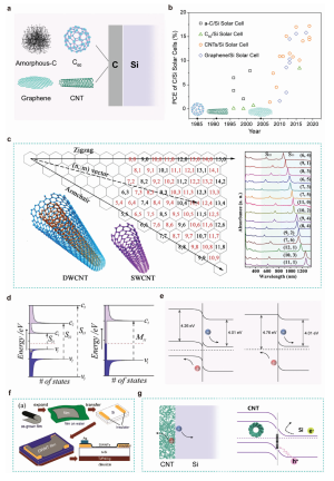
Similar to Si, carbon (C) is an abundant element in nature, and the exploration of carbon materials is closely connected to human history. Owing to their excellent carrier mobility, chemical stability, and optoelectronic properties, carbon materials fulfill all of the requirements for solar cell manufacture in combination with silicon.Generally, a C/Si HJ solar cell consists of a carbon layer (carrier-selective contact layer) and a Si (light absorbing layer) as well as front and rear metal electrodes. At present, the most common carbon films used in C/Si HJ solar cells are amorphous carbon (a-C), graphite, graphene, fullerene, and carbon nanotubes (CNTs) as shown in Figure 2a. The development of the C/Si HJ solar cells was initially slow due to the technical difficulties to integrate carbon materials. As such and until recently, the C/Si HJ device geometry was highly unusual when compared to commercial Si solar cells. In most cases, researchers employed an architecture resembling that of an organic solar cell with a window or frame-like geometry defined in the middle of a Si wafer. In this geometry, a SiO2/Si wafer was etched to reveal a small silicon opening in the SiO2 and the surrounding SiO2 was coated with metal electrode (such as Au, Ag, or Pt/Ti). The use of a window or frame like geometry allowed for the carbon film to be processed separately and later transferred to the window and this design was successful for many years. Figure 2b and Table 1 displays the representative results of window-like geometry C/Si solar cells from the year of invention to the year of 2019.

Figure 2. The characteristics of C/Si HJ solar cells. a) Four classes of carbon allotropes (a-C, fullerene (C60)), CNTs, and graphene) formation of C/Si HJ solar cells. Copyright 2015, John Wiley and Sons for Advanced Materials. b) The timeline exhibits the evolution and selected major events of C/Si HJ and solar cells up to 2019. c) Chiral map of SWCNTs. Zigzag and armchair nanotubes correspond to SWCNTs with m = 0 and n = m, respectively. Optical absorption spectra of different semiconducting SWCNTs achieved by sorting are presented on the right. S11 and S22 represent the first and second optical transitions of SWCNTs with the diameter ranging from 0.8-1.0 nm, respectively. Copyright 2020, John Wiley and Sons for Advanced Energy Materials. d) Schematic illustration of the DOS of s-SWCNTs (left) and m-SWCNTs (right) with the optical transitions between VHS.Copyright 2018, John Wiley and Sons for Advanced Energy Materials. e) The energy-band diagrams of the CNT/Si HJ solar cells based on p-n junction or Schottky junction solar cells.Copyright 2012, John Wiley and Sons for Advanced Energy Materials. f) Illustration of the fabrication process of DWNT/n-Si HJ solar cell.Copyright 2012, John Wiley and Sons for Advanced Energy Materials. g) The energy level diagram of C/Si HJ solar cells.
The use of nanomaterials offers a solution and work combining zero-dimensional fullerene (C60) in a (C60)/Si HJ has shown good rectifying properties, and by doping the C60 layer, surface passivation and the incorporation of anti-reflection coatings, a PCE of 8.43% (active area of 0.13 cm2) was achieved at a C60/p-Si solar cell by Yun et al. in 2016.However, the limited intrinsic conductivity of C60, makes the further development of the C60/Si solar cell challenging.
Although many technologies with electrical and optical design have been used to improve the CNT/Si HJ, two main limitations have hindered industrialization: the low PCE (<18%) and the small active area (<0.1 cm2) (as shown in Table 1). As shown in Figure 2f, the current method for preparing CNT/Si device with a window-like geometry involves conformally transferring CNT films to a Si wafer. The area of this architecture is usually small (0.008–2 cm2), and the design is difficult to scale up without compromising PCE. Furthermore, there are many defect states at the CNT/Si interface (Figure 2g), where recombination of the photoinduced carriers can lead to poor performance and interface passivation is key to achieving a high PCE. Currently, classic passivation (chemical passivation and field-effect passivation) techniques have been applied for high-efficiency Si solar cells. An alternative passivation strategy is chemical passivation (passivation materials including SiO2, a-Si:H) and is based on a covalent bond formed between the Si surface atoms and atoms inside the passivation materials; In contrast, field-effect passivation (such as Al2O3, SiNx) is linked to the use of an electric field provided by fixed charges in dielectric materials.The porosity of the CNT film made the use of traditional passivation layers like a-Si:H or SiNx difficult. Therefore, the existing passivation techniques are not compatible with the preparation strategy of CNT/Si solar cells. Moreover, the preparation of SiOx by thermal oxidation method requires a high-temperature process, and the preparation of Al2O3 or a-Si:H by PECVD requires high-vacuum equipment, which restricts the further reduction of crystalline silicon cell’s cost. To summarize, the window-like geometry architecture and the lack of suitable passivation techniques of CNT/Si HJ solar cells make it challenging to produce industrial-sized cells with PCEs above 20%. Therefore, a passivation method that can perfectly match this special CNT/Si HJ is highly desirable. Such a technique should; i) have a high passivation effect at CNT/Si interface; ii) have deposition conditions compatible with the CNT/Si interface; and iii) Ideally, integratable into CNTs themselves in a composite material.
上一篇: 一种高效的Ge(100)表面清洁方法
下一篇: 通过优化阴影蒸发技术改善晶圆尺度均匀性