ABSTRACT
Gallium Oxide (Ga2O3) is an ultra-wide bandgap semiconductor with a bandgap of 4.5–4.9 eV, which is larger than that of Silicon (Si), Silicon Carbide (SiC), and Gallium Nitride (GaN). A benefit of this ultra-wide bandgap is the high-temperature stability due to the low intrinsic carrier concentration. Another benefit is the high critical electric field (Ec), which is estimated to be from 6 MV/cm to 8 MV/cm in Ga2O3. This allows for a superior Baliga’s figure of merit (BFOM) of unipolar Ga2O3 power devices, i.e., they potentially can achieve a smaller specific on-resistance (RON,SP) as compared to the Si, SiC, and GaN devices with the same breakdown voltage (BV). The above prospects make Ga2O3 devices the promising candidates for next-generation power electronics.
This dissertation explores the design, fabrication, characterization, and packaging of vertical β-Ga2O3 Schottky barrier diodes (SBDs) and P-N diodes. The power SBDs allow for a small forward voltage and a fast switching speed; thus, it is ubiquitously utilized in power electronics systems. Meanwhile, the Ga2O3 power P-N diodes have the benefit of smaller leakage current, and the diode structure could be a building block for many advanced diodes and transistors. Hence, the study of Ga2O3 Schottky and P-N diodes is expected to provide the foundation for developing a series of Ga2O3 power devices.
In summary, this dissertation covers the design, fabrication, characterization, and packaging of Ga2O3 Schottky and P-N diodes, with the aim to advance Ga2O3 devices to power electronics applications. This dissertation addresses many knowledge gaps on Ga2O3 devices, including the voltage upscaling (ET), current upscaling (large-area device fabrication, packaging, and thermal management), and their concurrence (module demonstration), as well as the circuit-level switching characterizations.
On the horizon, Ga2O3 is an emerging semiconductor with an ultra-wide bandgap (UWBG) of 4.5–4.9 eV, which is higher than that of Si, SiC, and GaN. Benefitted from this larger bandgap, the theoretical performance of Ga2O3 power devices is superior to the Si, SiC, and GaN counterparts. Hence, Ga2O3 devices are regarded as the promising candidates for next-generation power electronics.
The power diode is an important component in power circuits, and the diode structure is usually a building block for power transistors. Small-area (0.1 A current level) Ga2O3 Schottky barrier diodes (SBDs) and P-N diodes are first designed and fabricated with a novel ET, the NiO JTE, reaching a high BV from 2.5 to 3.5 kV and junction E-field up to 4.2 MV/cm. Subsequently, large-area (>15 A current level) Ga2O3 diodes are fabricated with the same ET, achieving a BV of 1.6 kV, which is among the highest BV demonstrated in large-area Ga2O3 devices. In addition, on-wafer switching tests are performed on the medium-area (1 A current level) Ga2O3 P-N diodes, and their turn-on/off speed and reverse recovery time are comparable to commercial SiC Schottky barrier diodes.
1. Advantages and Challenges of Ga2O3 Power Devices
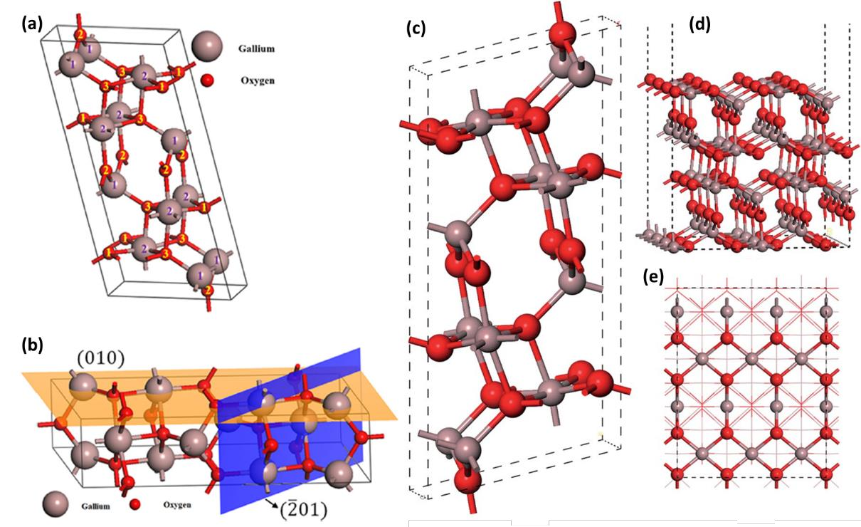
In the 1950s and 1960s, studies were conducted on bulk single crystals of Ga2O3. By the 1990s, advancements in melt and epitaxial growth technologies had been made. Recently, Ga2O3 has gained significant interest due to a breakthrough in material science, notably the substantial increase in substrate diameter and availability. Ga2O3 exists in five polymorphic forms identified as α, β, γ, δ, and ε . These forms include corundum (α), monoclinic (β), defective spinel (γ), and orthorhombic (ε), with the δ phase generally recognized as a variant of the orthorhombic phase . Figure 1-1(a) and 1-1(c) illustrate the unit cell structure of β-Ga2O3, and Figure 1-1(b) displays the (010) and (201) surfaces. Figure 1-1(d) and 1-1(e) depict the (100) plane. Among all these phases, the orthorhombic β-Ga2O3 structure is the most stable. Therefore, this research is centered on the monoclinic (β) structured β-Ga2O3 polymorph, which is the ideal material for power devices.

Figure 1-1. (a), (c) β-Ga2O3 crystal structure. (b) 010 and 201surfaces. (d) Crosssectional view of 100 surface. (e) Top view of 100 surface. In (c), (d), and (e), the Gallium atom is marked in gray and the Oxygen atom is marked in red.
1.1 Advantage 1: High Critical Electric field (Ec)
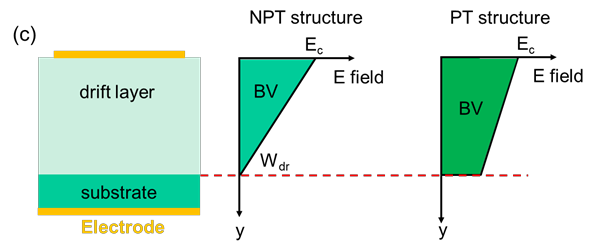
The primary advantage of using Ga2O3 material in power devices lies in its high critical electric field (Ec). In a vertical power device, the reverse-biased voltage is maintained within the drift layer, which is typically lightly doped and has a thickness ranging from a few micrometers (µm) to tens of µm. When the power device is reverse-biased, particularly for the widely adopted non-punch-through (NPT) design, the schematic of the E-field profile in the drift layer is shown in Figure 1-2(a).

Figure 1-2. (a) Profiles of the E-field inside a drift layer at a certain BV for the nonpunch-through (NPT) structure. Epeak location of (b) vertical Schottky barrier diode (SBD) and (c) vertical P-N diode.
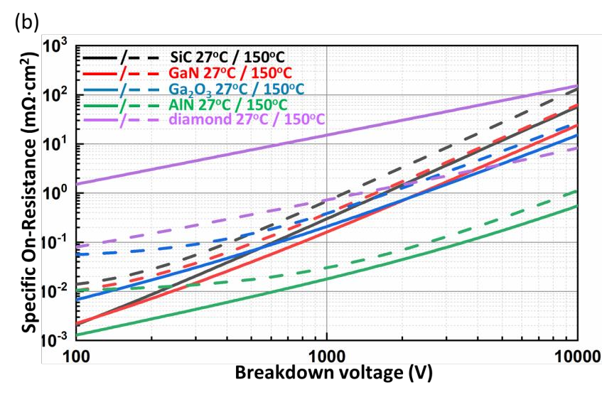
Figure 1-3(a) demonstrates that Ga2O3 exhibits a more favorable RON,SP ~ BV relationship when compared to SiC and GaN. Theoretically, under the identical BV conditions, a Ga2O3 power device can achieve a lower RON,SP compared to devices made of Si, SiC, and GaN. This advantage primarily stems from the high 𝐸c of Ga2O3.


Figure 1-3. Trade-off of breakdown voltage and specific on-state resistance in candidate materials for power devices. Punch-through design of the drift layer and incomplete ionization is not considered in (a), and considered in (b). (a) is adapted from. (c) E-field comparison between non-punch-through (NPT) and punch-through (PT) design of the drift layer.
上一篇: 微流控器件制造的双铸造方法比较
下一篇: 用于微系统异构集成的硅酸盐基封装材料