Abstract
3D heterogeneous integration (HI) and wafer-level packaging (WLP) represent the cutting edge of microelectronics design and fabrication. However, the current limitations of microelectronics packaging materials inhibit the widespread implementation of these processes, which presents an opportunity to develop new packaging solutions using innovative materials. Building upon previous work, research on the development and characterization of an improved silicate-based packaging material for 3D HI and WLP of microelectronics with a focus on Millimeter Wave (mmWave) radio frequency (RF) applications was carried out. A sodium-free material formulation and suitability with scalable deposition techniques demonstrated compatibility with complementary metal-oxide-semiconductor (CMOS) fabrication. The material was tested and qualified for use with common microelectronics fabrication processes such as positive and negative photolithographic patterning, wet etching, and most chemical cleans (excluding highly basic chemicals). It was polishable to a surface roughness of 197 ± 29 Å, thermally stable up to 400°C, compatible with high vacuum exposure down to 1.5 ± 0.4x10⁻⁵ torr, and filled gaps with aspect ratios as high as 18.6:1 using certain techniques. The packaging material could be deposited at thicknesses ranging from single-digit microns up to several millimeters, and exhibited excellent adhesion to silicon at thicknesses below ~30 µm. Residual stress generation in films of the silicate packaging material was less than 10 MPa at thicknesses of ~20 - 90 µm. The coefficient of thermal expansion was 2.968 ± 0.054 ppm/°C from 50 - 400°C, and the dielectric constant and loss tangent were ~4 and ~0.0002 at 110 GHz. Successful fabrication of a coplanar waveguide and prototype reconstituted wafers demonstrated that the packaging material can be used to make RF devices and to enable 3D HI and WLP.
Introduction
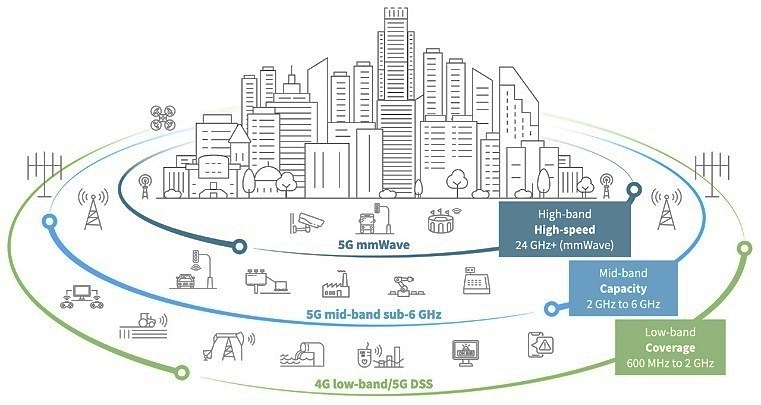
One promising way to address the issue of limited frequency space is through technological advancement. Previous technologies have left both commercial and government users unable to take full advantage of the higher frequency ranges of the RF spectrum. Figure 1 illustrates this range of frequencies, commonly known as Millimeter Wave (mmWave) or Extremely High Frequency (EHF) band. They extend from 30 to 300 GHz, have wavelengths from 1 cm to 1 mm, experience low signal latency, and offer high data transfer speeds ]. While they have limited range and can experience interference from physical objects (i.e. walls, buildings) or atmospheric effects (i.e. clouds, rain), they can be paired with existing long- to mid-range communications infrastructure to deliver the short-range, high-speed capabilities needed to enable the next generation of 5G/6G smart mobile devices, internet-of-things (IoT) architectures, and machine-to-machine (M2M) systems. Figure 2 shows a conceptual depiction of this interwoven communications landscape.

Figure 1. mmWaves occupy the high-frequency end of the radio spectrum

Figure 2. An interwoven communications infrastructure includes mmWave signals
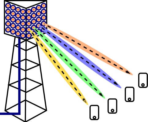
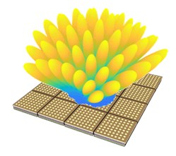
One of the key technologies that will enable this interconnected future is the phased array antenna. Phased array antennae operate using the principle of beamforming, which uses many small antennae to constructively interfere and produce an efficient, accurate, and precise signal. Phased array antennae also help counteract the extremely high signal attenuation present at mmWave frequencies. The closer together the radiating elements on a phased array are, the more precise the signal and the further the range of the antenna. However, each radiating element requires non-radiating support infrastructure; indeed, the higher the frequency generated the more supporting infrastructure is required. Typical microelectronics fabrication has primarily consisted of 2D architectures, but this imposes a limit on the minimum spacing between radiating elements, which has been a key factor limiting the manufacture of phased array antennae capable of operating at mmWave frequencies. In order to overcome the factors limiting antenna densification, new microfabrication strategies are needed. Figure 3 shows how phased array antennae can beamform precise signals, while Figure 4 shows a simulated RF signal produced by a phased array.

Figure 3. A phased array antenna can beamform signals directly to users

Figure 4. A phased array antennae producing simulated RF signals
3D Heterogeneous Integration & Wafer-level Packaging
Currently, many different microfabrication architectures exist from the purely two-dimensional to blended architectures to quasi-three-dimensional. Figure 5 shows some generic examples of what these pure and blended architectures look like in practice. On the left is a typical 2D architecture with silicon chips (or die) separately attached to the redistribution layer (RDL) via ball grid array (BGA). In the middle is a 2.5D architecture, where die are attached to a silicon substrate (commonly called an interposer) that also functions as a secondary RDL. Finally, the depiction on the far right shows 3D stacking of die using through-silicon vias (TSVs). This type of integration is currently used only for homogenous components (i.e. memory stacking), and is not yet viable for heterogeneous components due to practical challenges. Thus, a fully heterogeneous 3D IC remains beyond reach for now.

Figure 5. General architectures for 2, 2.5, & 3D integration
Deposition Methods
Various deposition methods were studied for the composite packaging material, with a particular focus on techniques that were highly scalable, economical, and easily integrable with microfabrication processes. The primary techniques studied were blade casting, spin coating, air spraying, ultrasonic spraying, molding, compression molding, and direct-write 3D printing. Graphical representations of each of the described techniques is shown below, accompanied by images of fabricated samples, a detailed description of how each method works, and their respective advantages and disadvantages.
Conclusions
3D HI and WLP represent the future in microelectronics design and fabrication. However, the limitations of current microelectronics packaging materials inhibit the implementation of these design and fabrication methodologies, and presents an opportunity for innovative solutions using novel packaging materials. This thesis documented research into an improved silicate packaging material for 3D HI and WLP of microelectronics with a focus on mmWave RF applications. The packaging material was shown to be CMOS-compatible due to its sodium-free chemical formulation, and achieved a ~103 reduction in binder sodium content compared to the previous sodium silicate binder without the use of cleanroom grade precursors or a contamination-free environment. The packaging material was processable with certain scalable deposition techniques (i.e. blade casting, molding) that are economically viable and integrable with CMOS processing. The chemical constituents of the silicate packaging material provide a significant cost-savings compared to other currently available packaging materials. The packaging material was compatible with many common microfabrication processes, including photolithographic patterning, wet etching, and most chemical cleans (excluding highly basic chemicals). It was polishable to an RMS surface roughness less than 500 Å, thermally stable up to 400°C, compatible with vacuum exposure up to HV, and could infill gaps with aspect ratios as high as 9.1:1 (blade casting with vacuum) or 18.6:1 (compression molding) depending on infill method. Thick film generation was possible on the order of 10s to 100s µm, and standalone parts were produced at thicknesses up to 5 mm. Adhesion of the packaging material to various substrates (unpolished/polished Si, PECVD SiO2 on GaAs) was acceptable for films less than ~30 µm in thickness. Residual stress generation in thick films of the packaging material was exceedingly low, with measured values of less than 10 MPa. The CTE of the silicate packaging material was closely matched to silicon, with a calculated value of 2.968 ± 0.054 ppm/°C. The dielectric constant and loss tangent were ~4 and ~0.0002 (at 110 GHz), respectively, qualifying the packaging material for use as a low-loss dielectric in mmWave RF applications. The material was successfully used to fabricate a simple RF device (CPW) and relevant architectures for 3D HI and WLP (prototype reconstituted wafers). Overall, the silicate packaging material represents a promising step forward in packaging solutions for 3D HI and WLP, particularly for mmWave RF applications.