The stability of long-term microfabricated implants is hindered by the presence of multiple water diffusion paths within artificially patterned thin-film encapsulations. Side permeation, defined as infiltration of molecules through the lateral surface of the thin structure, becomes increasingly critical with the trend of developing high-density and miniaturized neural electrodes. However, current permeability measurement methods do not account for side permeation accurately nor quantitatively. Here, a novel optical, magnesium (Mg)-based method is proposed to quantify the side water transmission rate (SWTR) through thin film encapsulation and validate the approach using micrometric polyimide (PI) and polyimide-silicon carbide (PI-SiC) multilayers. Through computed digital grayscale images collected with corroding Mg film microcells coated with the thin encapsulation, side and surface WTRs are quantified. A 4.5-fold ratio between side and surface permeation is observed, highlighting the crucial role of the PI–PI interface in lateral diffusion. Universal guidelines for the design of flexible, hermetic neural interfaces are proposed. Increasing encapsulation’s width (interelectrode spacing), creating stronger interfacial interactions, and integrating high-barrier interlayers such as SiC significantly enhance the lateral hermeticity.
1. Introduction
Microfabricated, polymeric neural interfaces have become increasingly popular in neuroscience and biomedical applications due to their engineered compliance, which helps minimize the mechanical mismatch between the implants and biological tissues.Compliance is achieved using thin (<10 μm thick) polymer substrate and superstrate (encapsulation), and embedded patterned metallic films. Despite numerous advantages, achieving long-term stability and reliable operation for such interfaces remain a challenge. The primary issue lies in the potential failure of the encapsulation layer, which can lead to leakages of body fluids and metal corrosion. Polymers often lack sufficient resistance to water ingress, and thin-film encapsulations, e.g., ceramic single-layer or multilayer, organic/inorganic multilayer, are not currently hermetic enough to sustain decade long exposure in vivo.
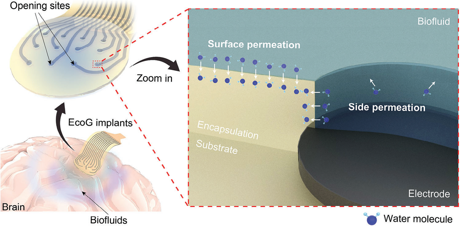
An electrode is a usual transducer in a neural implant: it is the prime tissue-device interface and is usually wired to an embedded metallic interconnect. Its design requires the encapsulation film to host an opening enabling tissue-electrode charge transfer. This results in multiple diffusion paths for water molecules: perpendicularly through the surface (surface permeation) and laterally through the exposed sidewalls and interfaces (side permeation) (Figure 1). The water transmission rate (WTR) usually refers to the surface permeation process and helps define the barrier performance of encapsulation films. With increasing number of electrodes and minimal dimensions, side permeation through the lateral portion of the encapsulation film should be monitored. The optical calcium (Ca) test enabled to evaluate the lateral water permeation in organic light-emitting diode (OLED) encapsulations, but its extreme moisture-sensitivity makes it incompatible with in vivo experiments. Mg films are a promising alternative, due to their sensitivity to water, visibility during the corrosion process, and compatibility with the process flow of minimized devices; so far only qualitative observations of surface permeation have been reported.

Figure 1. Multiple diffusion paths through a microfabricated electrode implant. Side permeation targets the walls of the patterned encapsulation film.
2. Results and Discussion
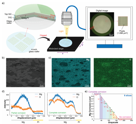
During corrosion, Mg visually switches from bright to dark gray,as a sign of water ingress. We design a microcell, in which a Mg disk (300 nm thickness, 0.5 mm radius) is laminated between 2 layers of 1 μm thick PI to mimic side permeation in standard PI-based flexible electrodes. 20 nm thick titanium (Ti) thin films are sputtered on the PI and the Mg to promote the PI-Mg adhesion and protect Mg from O2 plasma etching. The distance between the edges of the Mg disk and PI disk, named as width of encapsulation, is varied between 20 and 150 μm. A 400 nm thick SiC layer is deposited using plasma-enhanced chemical vapor deposition (PECVD) on the top of PI to suppress the surface diffusion in favor of the edge diffusion (Figure S1, Supporting Information). An array of 144 microcells with a range of geometries are produced on a flat, transparent glass wafer for constant and stable optical observation during monthly soaking in a 57 °C phosphate-buffered saline (PBS) solution. The PBS solution is replenished every week. Here, we elevate the temperature to 57 °C to accelerate the aging. The glass wafer is inverted onto a black polymethyl methacrylate (PMMA) substrate to eliminate the shadow effect of the top SiC layer (Figure S2, Supporting Information), then placed on a motorized stage with a resolution of 1 μm for automated positioning and capturing Mg images on a Leica DVM6 microscope in reflection mode. During the image capture process, the light emanating from the microscope’s lens travels through the glass wafer and the bottom PI layer before getting reflected off the Mg film, ultimately returning to the microscope’s lens. The resulting digital images (1600 × 1200 pixels) with each pixel of 1.096 μm2 surface area are recorded on a computer for further processing (Figure 2a).

Figure 2. a) Experimental setup of optical Mg test; the thin film encapsulation (TFE) may be PI or PI/SiC. b) SEM image and c) EDX map scans (Mg K𝛼 1, 2 and O K𝛼 1) of corroded Mg directly exposed to water vapor at 57 °C for 1 day. d) Through-thickness EDX line scan results for partially and wholly corroded Mg. e) The function of Mg corrosion levels and grayscale values.
3. Influence of SiC Interlayers on Side Permeation
Next, we introduce SiC interlayers into the system to enhance the overall lateral hermeticity. The high-barrier performance of PECVD SiC against water surface permeation has been con- firmed (Figure S1, Supporting Information). In this context, our focus shifts to investigating the water side permeation behavior through PI-SiC stacks. The Mg disks are sandwiched between two layers of PECVD SiC, each with a thickness of 130 nm; a thinner SiC film also covers the wall of the Mg disks. The remaining structure of the stacks follows the same design as that of the PI-Mg samples. We proceed to pattern the encapsulation layer widths to 20, 50, 100, and 150 μm, followed by immersing the wafer in a 57 °C PBS solution. We evaluate the Mg corrosion over time. Despite the SiC interlayer causing a slight darkening of the Mg color, determining the corrosion level based on grayscale remains feasible due to the persisting linear relationship between these two parameters (Figure S4, Supporting Information).
3. Conclusions
In conclusion, the proposed optical Mg test is a promising method for evaluating unprecedently water sideway diffusion in thin-film encapsulation. The nonuniform Mg corrosion limits the usage of binary images for further analysis. Nevertheless, digital grayscale optical micrographs enable to accurately quantify the surface and side water transmission rate, through a linear correlation between corrosion level and Mg grayscale value revealed by EDX analysis. The surface permeability of 0.17 g mm m−2 day−1 and side permeability of 0.76 g mm m−2 day−1 are measured separately for PI thin-film at 57 °C in PBS solution, the difference being attributed to the permeation of water molecules along the PI–PI interface. After an oxygen plasma treatment on PI–PI interface, the side permeability of PI is reduced to 0.35 g mm m−2 day−1. For PI-based devices with electrode patterns, the side permeation is likely to dominate encapsulation failure when the ratio of surface area to thickness is less than 4.5 (for weak PI–PI interface) or 2 (for robust PI–PI interface) times of the sidewall area divided by width. Introducing high-barrier inorganic interlayers can significantly decrease or slow down side permeation: SWTR is reduced from 38.99 (PI) to 2.41 (PI-SiC) g mm m−2 day−1 and lag time is extended from 0.7 (PI) to 20.8 (PI-SiC) days at 20 μm width. Even when the width of the SiC interlayer is reduced to an extremely small dimension (e.g., 130 nm), significant lateral hermeticity is likely to be achieved in PI-SiC system due to the observed trend of decreasing permeability with decreasing width. The stable electrochemical impedance observed over a 9-day period of soaking in 57 °C PBS for the 9 electrodes in the ECoG devices serves as validation for the adequate protection provided by the PI-SiC multilayer. The broad width of encapsulation, strong and robust interfaces and high-barrier inorganic that conformably covers the sidewalls of sensitive components are desired for designing hermetic neural interfaces. The optical Mg method is applicable for quantifying water side permeation in various thin- film barriers that are transparent to visible light, such as PI, Parylene C, PDMS, PET, Al2O3, TiO2, etc. However, barriers with opaqueness pose limitations to this method, and in such cases, the electrical Mg test can be employed to overcome this constraint.
4. Experimental Section
Microfabrication of PI-Mg-PI Disks for Side Permeation: The fabrication started with the pretreatment of 4 in. glass wafer. A glass wafer was cleaned with acetone and isopropyl alcohol (IPA) and activated by 600 W O2 Plasma (PINK GmbH Thermosysteme, V10-G) for 10 min, then adhesion promoter (VM652, 1 vl% VM651 diluted in IPA, HD MicroSystems) was spin-coated and dried at room temperature. Then 1 μm PI (HD Microsystems GmbH, catalog no. PI2610) was spin-coated on the pretreated glass wafer. 20 nm thick Ti layers were sputtered (AC450, Alliance-Concept) between PI and Mg as the adhesion layer. 300 nm thick Mg was thermally evaporated (E300, Alliance-Concept) as the humidity sensor. The 0.5 mm radius disks were patterned by the lift-off (10 mins 80 kHz/100% power ultrasonic bath in acetone). The other 1 μm PI layer was coated on top with/without O2 plasma (PINK, 200 W/2 min) pretreatment for robust PI–PI interface or weak interface. Then, a 400 nm thick PECVD SiC was deposited by Oxford PlasmaLab system 100 PECVD (133 sccm Ar, 60 sccm CH4, and 375 sccm 2% SiH4/Ar, 25 W, 300 °C, 30 min of deposition). The final etching step (Corial 210IL ICP-RIE etch system) patterned the stacks to 4 widths: 20, 50, 100, and 150 μm.
上一篇: GaN 半导体薄层电阻的宽带涡流测量
下一篇: 多晶钼纳米线的受控逐步湿法刻蚀