Abstract: Although the classical four-point probe method usually provides adequate results, it is in many cases inappropriate for the measurement of thin sheet resistance, especially in the case of a buried conductive layer or if the surface contacts are oxidized/degraded. The surface concentration of dislocation defects in GaN samples is known to challenge this kind of measurement. For the GaN sample presented in this study, it even totally impaired the ability of this method to even provide results without a prior deposition of gold metallic contact pads. In this paper, we demonstrate the benefits of using a new broadband multifrequency noncontact eddy current method to accurately measure the sheet resistance of a complicated-to-measure epitaxy-grown GaN-doped sample. The benefits of the eddy current method compared to the traditional four-point method are demonstrated. The multilayer-doped GaN sample is perfectly evaluated, which will allow further development applications in this field. The point spread function of the probe used for this noncontact method was also evaluated using a 3D finite element model using CST-Studio Suite simulation software 2020 and experimental measurements.
1. Introduction
The knowledge of the electrical conductivity of semiconductor materials has become a critical factor in the development of devices in the field of photovoltaic or power electronics applications. The need has, over the last decade, deeply increased with the demand for energetically efficient power components for computing, sustainable or grid applications. Gallium Nitride (GaN) has remarkable intrinsic properties, with a high thermal conductivity and a wide bandgap (3.4 eV), allowing it to have a high breakdown voltage, a high electron saturation speed and an increased energy density. It is consequently a semiconductor of choice when it comes to designing more efficient electronic structures such as field effect or bipolar transistors. Their reduced power loss, reaching up to 80%, emphasizes their economic interest for a large variety of applications. In both the scientific and industrial fields, great care is also paid to the purity and homogeneity of those materials before and during the manufacturing of a device.
The sheet resistance of the materials of interest is usually easily measured by a classical four-point probe measurement, but in some cases, this method fails to provide a measurement of the sample. If the contacts are too poor due to surface oxidation or inhomogeneous conductive layers caused by surface defects such as dislocations, or if the conductive layer of interest is buried under an insulating one, the current source will fail to apply the current needed to measure the contact.
2. Experimental Setup
In this section, the multifrequency eddy current experimental setup introduced in and used for the characterization of our GaN sample is described. This setup injects a broadband signal into a transmission line terminated by a probing coil. The coil, excited by an alternating signal, induces eddy currents within the conductive or semiconductor layer, leading to the generation of an induced magnetic field and a modification of the total magnetic field inside and around the layer (Figure 1). Consequently, the coil impedance changes according to the properties of the layer, such as its conductivity and thickness. The magnetic field is not affected by the presence of an insulating layer, which can be regarded as air (µr = 1). Therefore, the eddy current method can be successfully used to induce eddy currents in a conductive layer underneath an insulating one without being affected by the latter.
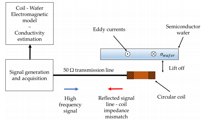
Figure 1. Experimental multi frequency eddy current (MFEC) setup. A multicarrier signal is sent and reflected at the coil-line impedance mismatch.
In this section, we were interested in determining the effective probing area of thekind of planar coil used since it was not previously evaluated and is an important factorto consider when dealing with small samples. This parameter is an important parameterThe point spread function (PSF), which can be directly related to the spatial distribution ofthe magnetic field generated by the coil is an important parameter to consider whendesigning and interpreting the conductivity of the sample measured. As shown in Figure 2 the magnetic field seen by the sample strongly depends on the lift-off. Consequently, thevalue measured would be an image of the conductivity of the probed area where the eddycurrents are induced. The probed area corresponds to the section of the PSF by a cuttingplane at a lift-off distance from the coil. Quite logically, considering the spatial extensionof the field, one would expect the PSF to be wider than the radius of the coil itself and to decrease in magnitude as a function of the lift-off, It is thus important to estimateits width compared to our coil to ensure that the effective pmbing section is not largelthan the sample itself. Otherwise, the analytical electromagnetic model used for fitting the conductivity may not be valid since it considers an infinite layer of conducting material. Ifthe magnetic field overlaps with the edges of the sample, the accuracy of the estimationwould be affected.
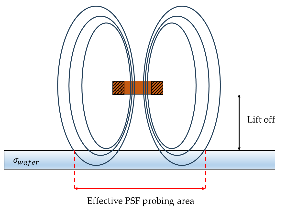
Figure 2. Schematic of the spatial distribution of the magnetic field over of a circular coil eddy current probe. The effective probing area of the sensor is directly related to the point spread function of the sensor inducing eddy currents in the sample under.
In this section, the coil probe structure presented in Figure 1 was modeled and simulated over the 1 MHz-1 GHz range in the air alone or with a sample for two lift-off valuesof 70 uum and 400 um. The 2D map of the magnitude of the magnetic field computed overthe coil in air alone is shown in Figure 3 for two lift-offs. Very interestingly, the associatedcut plots presented in Figure 4 for several frequencies show that the PSF has a very specific"M-shaped" structure caused by the air core and the small copper track width to coil radiusratio. As the frequency increases, the field is more closely localized at the surface of thecoil, and the field tends to be more homogeneous. In Figure 4, for a 400 jum lift-off, the fieldat the coil center is about 50% lower than the one above the copper track, while for a 70 umlift-off, the field is decreased by almost 90% and therefore mainly located above the coppertrack itself.
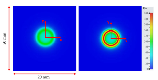
Figure 3. A 2D map of the magnetic the field magnitude, in air alone, for a (left) 400 um and (right)70 um lift-off at 1 Mhz.
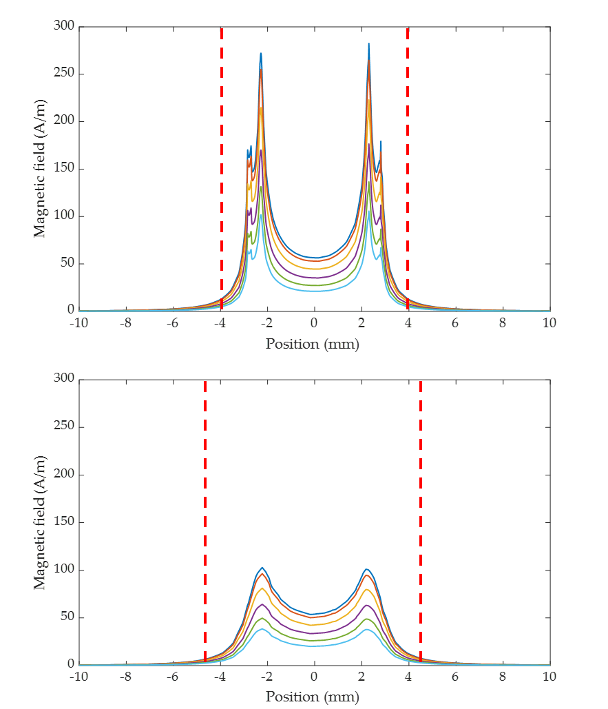
Figure 4. Plot of magnitude of the magnetic the field along the x direction, in air alone, for a lift-off of70 um (top) and 400 jm (bottom) over a 1 MHz-1 GHz range: (-) 1 MHz, (-), 200 MHz, (-) 400 MHz()600 MHz,(-)800 MHz (-)1 GHz.(--)90% field limit.
3. Experimental Result on the Measurement of a GaN Sample
GaN samples often contain surface dislocation due to the strongly different lattice constants and thermal expansion coefficients, as well as defects formed by lattice mismatch and residual impurities (C, O or N) . The GaN layers are therefore challenging to measure with a classical four-point probe because of their low contact quality without depositing metallic contact pads.
The sample we were willing to characterize and present in Figure 5 consists of three stacked layers of different doping concentrations. The top and inner layers of, respectively, 10 µm and 0.1 µm were grown by epitaxy on the free-standing layer of 300 µm. Their respective doping concentration were 2.1016 cm−3 , 2.1018 cm−3 and unknown. The sample side was a 12 mm × 12 mm square.
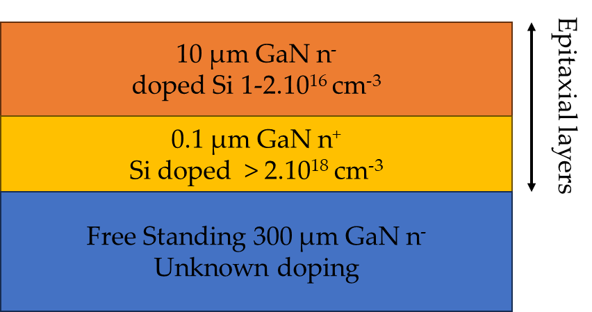
Figure 5. Structures and doping of the GaN sample layers deposited by epitaxy.
4. Conclusions
The development of efficient resistivity imaging capabilities is a must-have for the characterization process of semiconductors along the production chain. This paper shows the benefits of applying our patented broadband eddy current measurement method to the characterization of GaN, which was difficult to measure with a classical four-point probe hall method without having to realize the deposition of metallic contact pads. After recalling the measurement principle, it was shown how the method could satisfactorily measure the square resistance of a small, three-layer GaN sample grown and doped by epitaxy. Three-dimensional FEM simulations were realized in order to correctly estimate the probing section of the sensing coil utilized in order to ensure that no edge effects were impairing the measurement. The spatial extension of the point spread function of our eddy current sensors was characterized with respect to the radius of the coil. Finally, it was shown how the setup managed to precisely estimate its sheet resistance.
下一篇: 薄膜封装中水侧渗透的光学监测