Abstract: Graphene, renowned for its exceptional electrical, optical, and mechanical properties, takes center stage in the realm of next-generation electronics. In this paper, we provide a thorough investigation into the comprehensive fabrication process of graphene field-effect transistors. Recognizing the pivotal role graphene quality plays in determining device performance, we explore many techniques and metrological methods to assess and ensure the superior quality of graphene layers. In addition, we delve into the intricate nuances of doping graphene and examine its effects on electronic properties. We uncover the transformative impact these dopants have on the charge carrier concentration, bandgap, and overall device performance. By amalgamating these critical facets of graphene field-effect transistors fabrication and analysis, this study offers a holistic understanding for researchers and engineers aiming to optimize the performance of graphene-based electronic devices.
1. Introduction
Graphene has emerged as a promising material for next-generation electronics due to its exceptional electrical, optical, and mechanical properties. It possesses a honeycomb lattice structure of graphene, and its hexagonal shape corresponds to the symmetry of the graphene lattice in reciprocal space, as shown in Figure 1b,c. Specifically, graphene field-effect transistors (GFETs) have demonstrated the potential to outperform traditional silicon transistors in various applications such as flexible electronics, highfrequency devices, and sensors. However, realizing commercially viable GFETs requires overcoming significant fabricationchallenges related to scalability, reproducibility, and cost-effectiveness. This literature review provides a timely and in-depth analysis of state-of-the-art GFET fabrication processes and methodologies, focusing on addressing these aforementioned challenges through advanced materials engineering techniques and manufacturing approaches.
We systematically scrutinize critical facets of GFET development including graphene synthesis, transfer, and metrological assessments of quality. Recognizing that graphene’s pristine condition profoundly impacts device performance, we explore techniques to preserve superior electrical, structural, and quantum transport properties. Additionally, we delve into the intricacies of doping graphene to modulate its bandgap—an essential step in fabricating effective field-effect transistors (FETs). By examining various physical and chemical doping techniques thoroughly, we uncover their transformative impacts on electronic parameters and device behavior.

Fig1
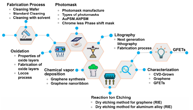
In this review, we systematically dissect the GFET fabrication process, as shown inFigure 2. Beginning with synthesis and transfer methods, we critically assess the state.of-the-art techniques that strive to preserve the intrinsic properties of graphene whileadapting it to scalable device architectures. The quality of graphene, being the linchpin ofdevice performance, necessitates rigorous evaluation. To this end, we examine a suite ofmetrology techniques, highlighting their insights into graphene's crystalline quality, defectdensity, and uniformity. Moreover, the intrinsic semi-metallic nature of graphene requiresa shift in paradigms to induce a controllable bandgap, rendering doping processes pivotalWe scrutinize the effects of various doping methodologies, from chemical to physicaadsorption and substrate-induced to electrostatic doping, detailing how each methodinfluences graphene's electronic, structural, and quantum transport properties. This reviewaims to provide a comprehensive resource for the graphene research community, facilitatingan understanding of the critical aspects of GFET fabrication and providing guidance forfuture innovations. Navigating these complex facets, we aim to articulate a clear pathtoward realizing high-performance graphene-based electronic systems.

Figure 2. The flowchart encapsulates the sequence of complex steps required to create GFETs discussed in this review, starting from the preparation of the substrate to the final characterization of the completed transistors. Each step is critical to the performance and yield of the GFETs.
2. Graphene Field-Effect Transistors
GFEls represent a groundbreaking advancement in nanoelectronics, leveraging graphene'sexceptional properties to revolutionize transistor technology potentially. Graphene exhibitsextraordinary electrical, thermal, and mechanical characteristics, making it an ideal candidatefor transistor applications. The core principle of a GFET lies in using graphene as the channematerial through which electric charge flows. Figure la illustrates a typical structure ofGFETsUnlike traditional silicon-based transistors, GFEls exploit graphene's high electron mobilityand ambipolar electric field effect. This results in transistors operating at higher frequencies andpotentially consuming less power: The high carrier mobility in graphene allows for faster chargetransport, contributing to the superior speed of GFEls compared to their silicon counterpartsAdditionally, because graphene sheets are so adaptable, they may be used to create transistors ona variety of surfaces, including flexible materials. This creates new opportunities for innovativeapplica tions of portable and wearable electronics. The potential for miniaturization beyond thelimits of silicon-based technologies is another compelling aspect of GFETs, aligning with theongoing trend of device miniaturization in electronics.
Astoundingly, a single gram of graphene possesses the capacity to span an entire football field, courtesy of its astonishingly low areal mass density of merely 0.77 milligrams per square meter. This remarkable attribute renders it exceedingly advantageous for producing transistors where material economy and lightweight characteristics are pivotal. The complex fabrication methodology for devising graphene-based devices encompasses a series of intricate steps, each contributing to the nuanced construction of these advanced components. This process is elucidated in detail within Figure 2, which serves as a cornerstone for the in-depth analysis presented in this comprehensive review.
3. Fabrication Process
3.1. Wafer Cleaning
Wafer cleaning, a process of paramount importance in integrating graphene into semiconductor devices, gains heightened significance due to the extraordinary sensitivity of graphene to surface contaminants. The exceptional electrical properties of graphene—properties that outstrip those of conventional semiconductor materials—are easily compromised by adsorbed molecules, which can scatter charge carriers and diminish the material’s intrinsic mobility. Thus, the presence of even monolayers of contaminants can lead to significant performance degradation in graphene-based components. The wafer cleaning process is a pivotal component in the semiconductor manufacturing workflow, essential for ensuring the integrity of microelectronic devices.
Graphene wafer cleaning is a critical process in the fabrication of graphene-based devices, and it varies significantly depending on the type of substrate used. Each substrate material presents challenges and requires tailored cleaning methods to ensure the integrity and quality of the graphene layer. The choice of the cleaning method directly impacts the electronic properties and performance of the final graphene devices, making the selection of an appropriate cleaning technique crucial for each substrate type. A deep understanding of the interaction between graphene and various substrates under different cleaning conditions is essential for optimizing the fabrication process and achieving high-quality graphene-based electronic devices.
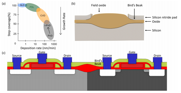
The concept of CVD for synthesizing graphene is not recent, with early experiments dating back to the 1970s. These early attempts aimed to understand the thermodynamics of monolayer and bilayer graphite growth on specific metal substrates like Ni (111) crystals. The CVD process involves the deposition of carbon atoms on metal surfaces using carbon sources such as CH4 gas, methanol, or polymethyl methacrylate (PMMA). The quality of CVD graphene depends on factors like reaction temperature (typically 800–1000 ℃) and vacuum levels . Afterward, CVD graphene can be transferred to various substrates following the chemical etching of the metal substrate. Several metals, including Cu, Co, Pt, Ru, and Ni, have been used as substrates, with Cu and Ni being the most employed. Cu substrates, in particular, tend to yield a higher proportion of single-layer graphene with larger grain sizes when compared to Ni substrates. Various methods of developing graphene are compared in Figure 3a.

Fig3
A recent study showed that the cold wall CVD approach enables unparalleled control of process parameters such as gas flow rates, temperature, and pressure. As a result, it may be utilized to examine the underlying surface science involved in graphene nucleation and growth. The research was conducted in a vertical cold wall system made at home that used resistive heating by running a direct current through the substrate. It gave a clear understanding of the usual surface-mediated nucleation and growth mechanism in two-dimensional materials generated by catalytic CVD under conditions desired by the semiconductor industry.
3.2. Photolithography and Electron-Beam Lithography
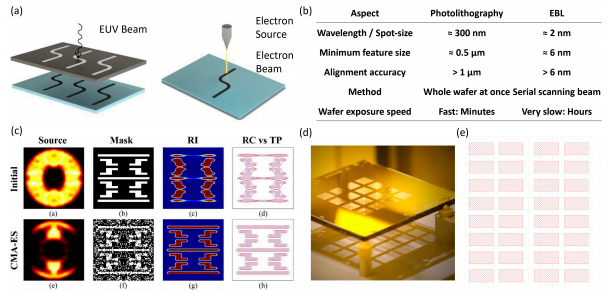
Photolithography and electron-beam lithography (EBL) are pivotal in fabricating and patterning graphene-based devices, each offering distinct advantages and constraints. Figure 4a demonstrates the working principle for EBL and photolithography, and Figure 4b compares the figure of merit of both methods. Photolithography, traditionally used in semiconductor manufacturing, can achieve feature sizes in the sub-10-nanometer range with advanced techniques like extreme ultraviolet (EUV) lithography. This resolution is generally sufficient for a wide range of GFET applications. The primary limitations of photolithography include its diffraction limits and the complexities associated with smallerscale patterning. On a very small scale, photolithography may struggle to maintain accuracy and uniformity. Additionally, the cost of high-resolution photolithography, especially with EUV lithography, is significant: techniques such as computational lithography shown in Figure 4c and multiple masks with different diffraction corrections shown in Figure 4d need to be implemented, potentially impacting the economic viability of GFET production.

Fig4
On the other hand, EBL employs a focused beam of electrons to write intricate patternson an electron-sensitive film directly, excelling in high-resolution fabrication essential foradvanced nanoscale graphene devices. It is a maskless operation, and we only need todesign a GDS file, as shown in Figure 4e, giving outstanding flexibility, It offers unmatchedprecision, crucial for the research and development of new graphene technologies, butis generally slower and less suited for mass production, with higher costs due to thecomplexity and precision of the equipment. The choice between these two techniqueshinges on the specific requirements of the graphene device, such as the desired resolutionproduction scale, and pattern complexity. In some instances, both methods are combinedwith photolithography used for overarhing large-scale patterning, while EBL is reservedfor finer, more complex features. Thus, photolithography and EBL are integral to thegraphene fabrication process, each contributing uniquely to the field's advancement andthe realization of innovative graphene-based technologies.
4.Conclusions
Graphene’s unique crystalline and band structure imparts extraordinary electrical, optical, and mechanical properties. In this comprehensive review, we explored the multifaceted aspects of graphene transistor technology, emphasizing the nuanced balance of parameters necessary for optimizing GFET production. Key findings highlighted the significance of the cleanness of all surfaces, graphene fabrication and transfer, oxide selection and parameters, and characterization in achieving high-performance transistor fabrication. Additionally, we explored the detailed aspects of doping graphene and analyzed how it influences its electronic properties. This investigation revealed how these dopants significantly alter the charge carrier concentration, bandgap, and overall performance of devices.
上一篇: 多晶钼纳米线的受控逐步湿法刻蚀
下一篇: 蚀刻对薄膜单晶铌谐振器的影响