Abstract. A single crystal niobium thin film was grown using molecular beam epitaxy on a c-plane sapphire wafer. Several samples were fabricated into dc resistivity test devices and coplanar waveguide resonator chips using the same microfabrication procedures and solvent cleans. The samples were then subject to different acid cleaning treatments using different combinations of piranha, hydrofluoric acid, and buffered oxide etch solutions. The different samples expressed changes in dc resistivity in the normal and superconducting states such that the low temperature resistivities changed by more than 100%, and the residual resistivity ratio dropped by a factor of 2. The internal quality factor of coplanar waveguide resonators measured near 5 GHz also showed significant variation at single photon powers ranging from 1.4×10⁶ to less than 60×103 . These changes correlate with the formation of surface crystallites that appear to be hydrocarbons. All observations are consistent with hydrogen diffusing into the niobium film at levels below the saturation threshold that is needed to observe niobium hydrides.
1. Introduction
The elementary components of superconducting qubits are capacitors, inductors, and Josephson junctions. The composition of these various elements allow one to create different anharmonic resonant circuits, from a simple transmon, conceptualized as a single Josephson junction shunted by a capacitor, to more exotic circuits with more Josephson junctions.
While the dc dissipation of the elements that make up the circuits is nominally zero, the rf or microwave dissipation is finite and ultimately limits the coherence of the device. For material sources of loss, the two leading candidates are dielectric and quasiparticle loss. In consideration of dielectric loss, all materials in proximity of the electric field can contribute. Superconducting quantum circuits are fabricated with careful selection of lowloss substrates such as sapphire and float-zone refined silicon, and thin film superconductors that form oxides and substrate interfaces that are low loss. Fabrication hygiene is also important as residual resist from fabricating the circuits can limit the lifetime of the qubit. Therefore, there is great interest in the materials and details associated with high-quality thin superconducting films with minimal oxide, defect, and interfacial losses and the processing of these materials into lowloss devices.
Superconducting Nb has been studied extensively for use in radio frequency cavities that are a critical component for particle accelerators and a robust methodology has been established to minimize surface resistance. Some of these treatments include vacuum annealing to modify the native oxide composition. Hydrogen incorporation is also a concern as it has been shown to be highly diffusive, can form defects, and modify the low-temperature electrical resistance.
2. Thin film growth, processing, and cleaning
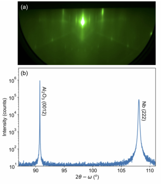
Reflection high energy electron diffraction (RHEED) was collected after the wafer was cooled to 200 ◦C. The pattern in figure 1(a) shows a streaky 3x pattern indicating an ordered Nb surface. The symmetric x-ray diffraction measurement shown in figure 1(b) only shows peaks associated with sapphire {0001} and Nb {111} planes. The strong intensities indicate that the film has a high degree of uniformity and that Nb (111) is parallel to Al2O3 (0001). The Nb (222) Peak at 2θ − ω = 108.095◦ is nearly completely relaxed with a residual biaxial in-plane strain of ϵx = −9.26 × 10⁻⁴ .

Figure 1. (a) Post-growth, in-situ reflection high energy electron diffraction pattern from the single crystal niobium thin film. (b) x-ray diffraction ω − 2θ measurement of the as-grown single crystal niobium film on sapphire.
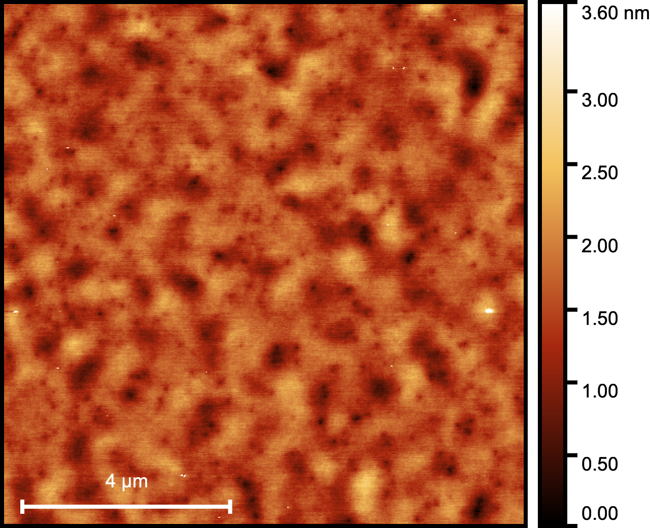
The surface topography is measured by AFM and shown in figure 2. The 10 × 10 µm scan exhibits a root mean square roughness of 328 pm, peak-to-peak roughness of 10 nm, and extrapolated autocorrelation length of 238 nm.

Figure 2. A 10 × 10 µm topographic atomic force microscope measurement of the niobium (111) surface before processing the film.
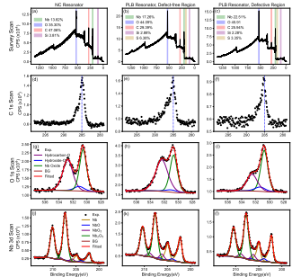
In comparison, the NC sample survey scan (figure 3(a)), exhibits silicon and carbon contamination, but not sulfur contamination. Furthermore, the carbon contamination is significantly larger compared to either region of the PLB sample. The Nb is also more fully oxidized (figure 3(j)), with lower proportions of suboxides and metallic Nb. The O 1s hydrocarbon peak is more separated and prominent compared to the niobium oxide peak.

Figure 3. X-ray photoelectron spectroscopic data for the three measured areas: the NC resonator (first column), the defect-free region of the PLB resonator (second column), and the defective region of the PLB resonator (third column). We include the survey scan ((a)-(c)), as well as the C 1s ((d)-(f)), O 1s ((g)-(i)), and the Nb 3d ((j)-(l)) scans for each area being scanned. Rows share the same legend.
3. Discussion
The methodologies applied in this study have not identified direct evidence linking hydrogen to the composition or electrical differences between the samples. Nor has the acid clean treatments been optimized to maximize the observed quality factor of Nb resonators. Instead, the context and consistency of the reported observations suggest that hydrogen incorporation is likely occurring during HF acid treatments. The single crystal nature of the studied film provides opportunities to observe these interactions in a different perspective than previous studies of polycrystalline Nb.
4. Conclusions
The single crystal niobium thin film grown on a c-plane sapphire wafer was fabricated into devices and subject to several acidic clean treatments that express differences in the dc resistivity in the normal and superconducting states, as well as significant reduction of the internal quality factor of coplanar waveguide resonators measured near 5 GHz. These changes correlate with the formation of surface crystallites that appear to be hydrocarbons. All observations are consistent with hydrogen diffusing into the niobium film at levels below the saturation threshold that is needed to observe niobium hydrides. Further studies are required to determine optimum etch procedures when using dilute HF solutions.
上一篇: 石墨烯晶体管的综合研究与设计