The megachip approach helps to rearchitect heterogeneous chip tiling for developing highly complex systems having desired circuit density and performance. Recent work on large-area superconducting integrated circuits to join multiple individual die is highlighted in this article, with particular attention paid to the processing of the highdensity electrical interconnects formed between the individual die. A variety of megachip assemblies were fabricated and characterized using several techniques (i.e., scanning-electron microscopy (SEM), optical microscopy, confocal m icroscopy, X-ray) to i nvest igate t he i nteg rat ion qu alit y, m i n i mu m feature size, silicon content, die-todie spacing, and gap filling. Silicon dioxide, benzocyclobutene (BCB), epoxy, polyimide, and silicone-based dielectrics were used for gap fill, via formation and redistribution layers (RDLs).
Introduction
The increasing demand for digital computing, mobility, and connectivity is driving the microelectronics industry toward cost-driven, highlyintegrated, miniaturized technology with increased performance and lower power consumption to bring nextgeneration devices into more and more applications. Over the last decade, high-performance computing (HPC) has evolved to adapt smaller and more diverse technology nodes suitable for artificial intelligence (AI), machine learning, and embedded computing platforms—these applications consistently involve tradeoffs between enabling more compute capability versus constraints in volume, weight, power, and thermal management.
Conventionally, better wiring densities have been achieved by using filled dielectric to reduce via dimensions, lines, and spaces—thereby increasing the number of circuit layers — and utilizing microvias for interconnection. However, each of these methods has inherent limitations. For example, there are limitations related to laser drilling and electroplating of high aspect ratio blind- and through-vias, increased resistance of narrow (and) long circuit lines, and increased cost of fabrication related to additional wiring layers. As a result, microelectronics packaging is moving toward alternative, innovative, low-cost approaches as solutions for miniaturization. Fabrication, assembly, and heterogeneous integration are bridging the gap by enabling economic use of the third dimension (2.5D and 3D packaging). System-level integration is also emerging. These approaches include multi-die system-on-chip (SoC), systemin-package (SiP), stacked die, or packagestacking solutions.
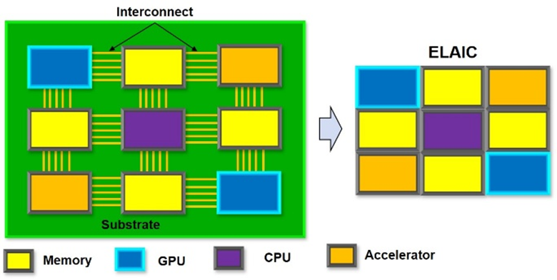
The ELAIC integration process willallow the tiling of known-good chipsto make systems that perform as asingle-chip monolithic device, despitebeing composed of several smallerheterogeneous chips. The primary goal ofthis effort is to develop a chip packaginginterconnected with a RDL that iscapable of integrating hundreds of chipsin proximity to one another in a singlesystem as shown in Figure 1. The RDLtypically has multiple metal layers, eachseparated by a plasma-enhanced chemicalvapor deposition (PECVD) silicon dioxidelayer, polyimide, or BCB dielectric, anduses micro-vias for interconnection.For our demonstration,the metalwiring layers were patterned using non-contact direct-write photolithographywhich supports minimum wiring layerdimensions of lum and field sizesexceeding the largest relevant reticle size(50 x50mm').

Figure 1: Extremely large-area integrated circuit (ELAIC), or megachip, concept: a) (left) Regular package where individual chips are attached to the substrate (organic or Si) and interconnected through the substrate; b) The megachip combines all the chips in a single plane where each individual chip will have at least two nearest neighbor chips for interconnection. The megachip enables chip-like wiring and eliminates the need for a substrate containing interconnects.
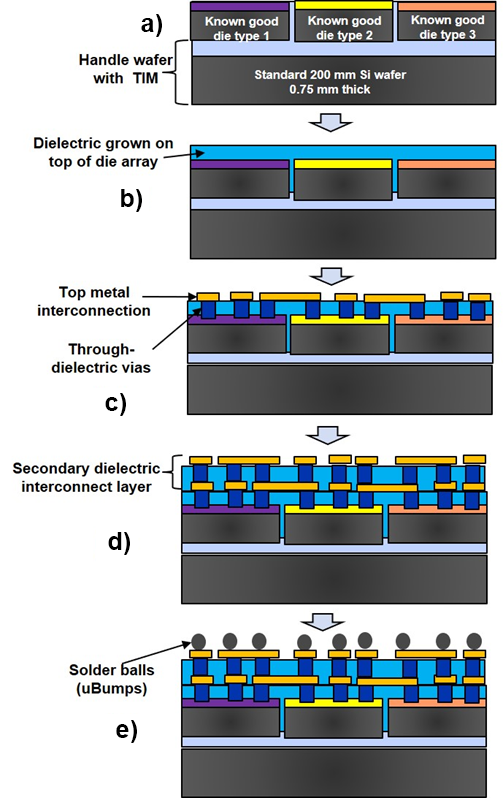
We evaluated various chip-likedielectric, wiring, and interconnectionoptions. An ELAIC process flow isillustrated in Figure 2. The illustrationdisplays the process flow for a double-layer RDL with a micro-bump layer ontop of the RDL. The primary advantageof the ELAlC assembly is to produce anarrow (5-20um) gap between the chips. This kind of gap is suitable for short (50 to500um) chip-to-chip interconnect lengthsas shown in Figure 2c.

Figure 2: Process flow for an ELAIC construction. The chips are assembled on a handle wafer: a) Knowngood die are placed face-to-face using a microscope. In general, the die use thermal interface materials (TIM) or related materials for die attachments; b) The dielectric layer is deposited; c) The first RDL is formed; vias are etched and top metal is deposited on the dielectric layer; d) The second RDL and additional dielectric layers for more complex interconnectivity are formed (target up to 4 RDLs); and e) Micro-bump fabrication—the bumps are deposited for flip-chip connection.
As a first step for chip tiling, wedeveloped an assembly process formaintaining narrow gaps between thechips while maintaining top chip surfaceplanarity in a larger scale ELAlC format.The top chip surface planarity enablesthin dielectric deposition to make afiner pitch interconnection with chip-like RDL circuits, We assembled variousELAlC configurations using smm x5mm to 20mm x 20mm chips in orderto test chip surface planarity and chip.to-chip spacing/gap for the ELAICstrueture, Figure 3 shows various ELAICconfigurations using $mm by Smm chipsranging from 4 chips up to 256 chips asa representative example.

Figure 3: The ELAlC combines known-good dietogether to make systems that perform like anextremely large single chip. The scalability ofthe ELAlC fabrication process is shown-withassembly slzes ranging from 4 chips to 16 chips to256 chips: a) Four 5mm x 5mm chip assembly; b)16 5mm x 5mm chip assembly; and c 256 5mm x5mm chip assembly.
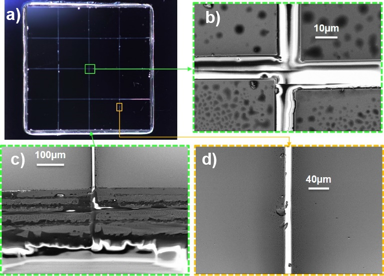
We used a variety of nondestructive analysis techniques for ELAIC physical device characterization. Figures 4-5 show representative examples of ELAIC characterization. SEM, confocal scan, X-ray, and optical images are used to characterize key fabrication steps, which include chip-to-chip spacing, interchip planarity, dielectric deposition, via formation, feature size, and microbumping. Figure 4 shows spacing between the stealth-diced chips in a 16- chip ELAIC assembly. The SEM data indicates that the ELAIC fabrication process maintains a narrow gap of 5-20µm between the chips and gap filling between the chips. Appropriate cleaning to remove dicing debris and give a smooth chip edge with minimal chipping is critical for minimizing chipto-chip spacing.

Figure 4: A 16-chip ELAIC assembly with very small 5-20µm chip-to-chip (C2C) spacing filled with dielectric. a) (top left): optical image of a 16-chip (each 5mm x 5mm) ELAIC assembly and b-d) (top right, bottom left, bottom right) corresponding enlarged SEM images that indicate a narrow C2C spacing filled (white area in SEM) with dielectric.

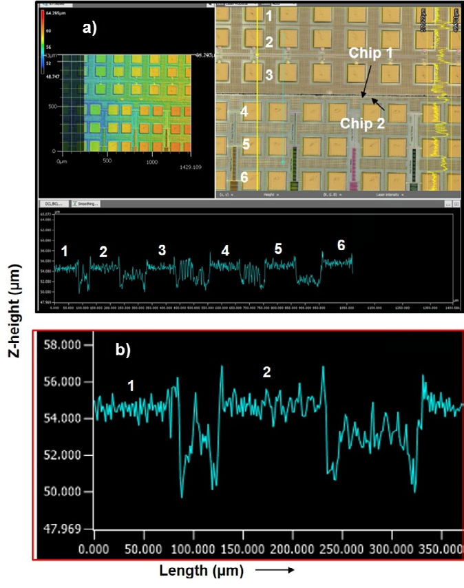
Figure 5: Selective-area confocal scan for a 4-chip ELAIC assembly. The figure shows confocal images and corresponding line scan between the chips to measure inter-chip planarity: a) Confocal micrograph and corresponding line scan. Confocal line scan from chip 1 metal pads (1,2,3) to chip 2 metal pads (4,5,6); and b) An enlarged confocal line scan; the confocal line scan shows metal pad height variation along the line as it scans from one edge to the other.
Summary
An integrated approach to develop ELAICs, or “megachips,”using varlousheterogeneous die configurations has beendemonstrated, This approach is suitablefor high-end, expensive electronies wherean SoC can be divided into chiplets withdesired functionality and an ELAICmulti-die SoC can be created. The ELAICcan incorporate chips/chiplets fromdifferent foundry processes, and differenttechnology nodes to improve mix andmatch capability, which further improvespackage performance, It also providesscalability to place a large number ofchips onto the ELAIC platform, andenables a design that packages manydifferent functionalities together, making it a viable approach to build largersystems.
The ELAlC solution is suitable formaking the right choices in terms ofcost and partitioning for each of thetargeted applications, and to providea heterogeneous path for large-scalefabrication. The ELAlC integrationsupports the capability to integratehundreds of chips (also known as chiplets)in proximity to one another in a singlesystem. This integration technologyenables small (50-100μm)interconnectsrequired for parallel interfaces for chip.to-chip communications, The extremelylarge area integrated circuit allows forconnections between bare chips, and thewiring between chips to be as small asthe wiring within a chip. The approachinereases the circuit complexity that canbe integrated within a given space byenabling sufficiently high chip-to-chipconnectivity to allow multi-chip systemsto perform as a single-chip monolithicdevice.
上一篇: 先进的氮化镓衬底化学机械抛光技术
下一篇: 用超薄钐层钝化多晶铜