Herein, it is reported that how a layer of samarium (Sm) with a thickness equivalent to ≈2 atoms (0.8 nm) deposited by thermal evaporation is remarkably effective at passivating polycrystalline copper (Cu) toward oxidation in ambient air. To monitor the rate of Cu oxidation in real time, slablike Cu films with a thickness of 9 nm are fabricated on glass modified with a layer of 3-mercaptopropyl silatrane, which immobilizes condensing Cu atoms by reaction with the thiol moiety, promoting slablike film formation at very low thickness. Upon exposure to ambient air the rate of increase in electrical resistance due to reaction with oxygen and water is slowed by more than an order of magnitude when the Cu film is capped with the ultrathin Sm layer. After 1 year, the resistance increases by ≈30% as compared to ≈190% for Cu films without an ultrathin Sm layer. Photoelectron spectroscopy, atomic force microscopy, and Kelvin probe measurements shed light on the underlying mechanism of passivation. Additionally, the ultrathin Sm layer is greatly lowering the work function of polycrystalline Cu films making this approach attractive for applications requiring a low-work-function electrode with high stability in air.
1. Introduction
Copper (Cu) is the electrical conductor of choice for the electronics industry because it is inexpensive compared to the other most conductive metals, gold and silver.Due to the demand for miniaturization of integrated circuits to enable increased computing power, the dimensions of Cu interconnects in integrated circuits are now below 100 nm.At the same time, nanostructured Cu is increasingly of interest for a wide range of emerging technologies, including next-generation photovoltaics, lightemitting diodes,sensors, printed electronics,high-frequency tags, nano-generators, and wearable electronics.Cu is considered relatively stable toward oxidation in ambient air because, after the formation of the few nanometers of surface oxide (which occurs in the first few hours) the oxide layer thickness increases very slowly. However, the properties of nanostructured Cu such as ultrathin films, nanowires, nanoparticles, grids,and nanofibers are all very sensitive to the extent of surface oxidation because 1) the oxide layer consists mainly of copper (I) oxide (i.e., Cu2O) and copper (II) oxide (i.e., CuO), which have electrical conductivities orders of magnitude lower than the base metal and 2) a surface layer a few nanometers thick can constitute a significant proportion of the total volume of nanoscale objects. While device encapsulation can slow the ingress of oxygen and water it can rarely completely block it so it is important to identify ways to slow the oxidation of nanoscale Cu in air without electrically isolating it from its surroundings. In recent years, there have been several high-profile reports relating to strategies for slowing Cu film oxidation, including using an atomically smooth Cu surface and passivating with an ultrathin surface-coordinated organic layer.
2. Results and Discussion
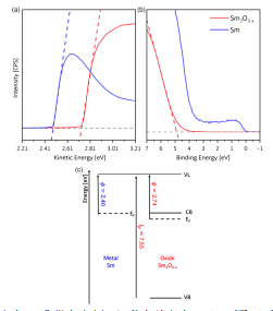
Given the large negative Gibbs free energy of formation of Sm2O3,-1734.6 kJ mol-1 , a Sm film only 0.8 nm (≈2 Sm atoms) in thickness would be expected to oxidize very quickly in ambient air. To confirm this, before considering the special case of 0.8 nm Sm on Cu, the ϕ of an evaporated Sm film 20 nm in thickness with and without exposure to ambient air for 15 min was measured using ultraviolet photoelectron spectroscopy (UPS) and the Kelvin probe technique. For solids, the mean-free path of photoelectrons excited with ultraviolet light is of the order of 1 nm, so provided ≥1 nm of the Sm-filmoxidized UPS measures the ϕ of the oxide rather than that of the underlying metal with modified surface potential.The ϕ of Sm and Sm2O3 measured using UPS is 2.4±0.1 and 2.7 ± 0.1 eV, respectively (Figure 1a), which agrees with the literature values for Sm and Sm2O3 of 2.4 and 2.7 eV.The ϕ of Sm and Sm2O3, measured using the Kelvin probe technique is 2.4±0.1 and 2.8±0.2 eV respectively, which is the same (within error) as that measured using UPS. Since the Kelvin probe technique measures the average ϕ under a gold mesh electrode of area 9 mm2 and UPS measures the lowest ϕ, the agreement between measurements made using these two different techniques indicates that the ϕ varies uniformly across both the metal and its native oxide (i.e., there is no significant nanoscale/micron scale heterogeneity).

Figure 1. a) Secondary-electron cutoff and b) valence band edge regions of the ultraviolet photoelectron spectroscopy (UPS) spectra of Sm (blue) and Sm oxide (red) films after Arþ sputtering to remove surface contamination. c) Energy level diagram summarizing the information extracted from the UPS spectra together with the bandgap of polycrystalline Sm2O3 reported in Ref.
Having confirmed that a Sm film with thickness equivalent to 0.8 nm would be expected to oxidize very quickly upon exposure to the ambient air, the next stage was to assess its ability to passivate Cu. To monitor the rate of Cu oxidation in real time, slablike Cu films with a thickness of 9±0.5 nm (equivalent to ≈35 Cu atoms) were fabricated on glass. At such low Cu thickness, the electrical resistance can be used as a direct measure of the extent of oxidation of the film surface provided the film is of uniform thickness (i.e., slablike). Due to the high surface energy of Cuand its tendency to diffuse, even at room temperature,fabricating Cu films of uniform thickness at such low metal thickness is difficult. To ensure that the 9 nm Cu film is compact and slablike, the glass substrate was first treated with a thin layer of 3-mercaptopropyl silatrane (MPS) to seed Cu atom condensation, as detailed in Experimental Section and Figure S2, Supporting Information. The uniform thickness of Cu films deposited on MPS-modified glass is evident from the crosssectional transmission electron microscopy (TEM) images shown in Figure S3, Supporting Information, from which it is evident that the film is polycrystalline with crystallite sizes of the same order as the film thickness. Analysis of the films with and without an MPS seed layer using grazing incidence small angle X-Ray scattering (GISAXS) reveals that Cu films on glass derivatized with MPS have a substantially smaller mean crystallite radii than on glass alone, 62 versus 76 Å (Figure S4, Supporting Information). The root-mean-square roughness of the Cu films on glass modified with MPS, measured using atomic force microscopy (AFM), is also reduced as compared to that on glass from 926±7 pm to 679±12 pm (Figure S5, Supporting Information). Taken together the TEM, GISAXS, and AFM measurements show that the MPS layer serves to immobilize the condensing Cu so that for a metal thickness of 9 nm a compact, slablike film is formed as Figure 2a, which serves as a convenient research tool for monitoring the rate of surface oxidation over long periods. Notably, while it is known that MPS can be used as a seed layer for the formation of compact silver films, to our knowledge, there are no published reports of it being used as a nucleation layer for Cu films.

Figure 2. a) A schematic 3D representation of a 9 nm Cu film with 0.8 nm Sm capping layer supported on an 3-mercaptopropyl silatrane (MPS)-derivatized glass. b) Evolution of sheet resistance with time in ambient air for 9 nm Cu films supported on MPS derivatized glass with and without 0.8 nm Sm capping layers.
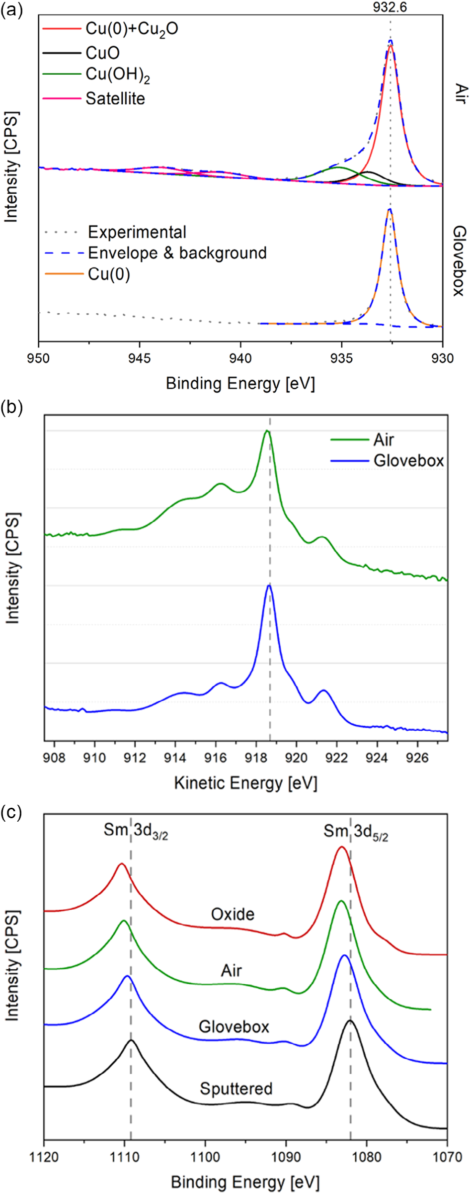
X-ray photoelectron spectroscopy (XPS) was used to provide information about the chemical state of the Cu and Sm components after 14 days storage in a nitrogen-filled glove box (<5 ppm oxygen and water) and after exposure to the ambient air. For the sample stored under nitrogen, the spectra in Figure 4 show no evidence of Cu oxides, since there is no chemical shift in the Cu 2p3/2 peak (which is well fitted with a single peak) and there are no satellite peaks. Additionally, the line shape of Cu Auger LMM region is consistent with that previously reported for pristine Cu. However, there is an evidence of partial oxidation of the ultrathin Sm layer, since the Sm 3d peaks are shifted to higher binding energies. While the oxygen partial pressure in the glove box is small, it is significant, so oxidation of the metal films is still expected to proceed very slowly. At face value, it could be concluded that this result is consistent with Sm forming a continuous layer over the Cu surface and reacting with incident oxygen molecules forming a compact Sm oxide layer that impedes oxidation of the underlying Cu. However, Kim et al. have recently shown that the close packed Cu (111) surface can be extremely resistant to oxidation in ambient air when step edges on the surface are no more than monoatomic in height.Conversely, at the multiatomic step edges prevalent at the edges of metal crystallites, oxidation proceeds rapidly. An explanation that is consistent with the aforementioned AFM measurements and electrical measurements is that Sm has accumulated at the boundaries between the Cu crystallites where it reacts with oxygen to form an oxide plug that hinders oxygen and water to those parts of the Cu crystallites most susceptible to oxidation (i.e., the crystallite boundaries).

Figure 4. Photoemission and Auger emission data of Cu|Sm electrodes stored in different conditions (ambient air and glove box) and reference Sm2O3–x and Sm metal film Ar ion sputtered for 20 min. a) Fits for highresolution X-Ray photoelectron spectroscopy (HR-XPS) scans of Cu 2p3/2 region. b) An overlap of normalized scans of Cu LMM Auger regions. c) Normalized XPS Sm 3d spectra with reference lines at 1083 and 1109.2 eV.
3. Conclusion
In summary, we have shown that a Sm layer with equivalent thickness equal to 0.8 nm deposited by simple thermal evaporation is remarkably effective at stabilizing polycrystalline Cu films toward oxidation in ambient air. Collectively the experimental evidence shows that the Sm atoms aggregate in the topographic and energetic well between crystallites in the Cu film during Sm deposition. Upon exposure to ambient air, the Sm is oxidized to Sm2O3–x (where x< 1), which retards oxidation by blocking the approach of oxygen to the multiatomic step edges at the crystallite boundaries. The heterogeneous distribution of this passivating oxide layer combined with its very low thickness ensures that the underlying Cu metal is not electrically isolated, and so this simple passivation step renders Cu films stable for transparent electrode applications in emerging optoelectronic devices.
上一篇: 异构小芯片集成以制造大型芯片
下一篇: 用于硅片翘曲估计的多步机械和热均质化