Abstract: In response to the increasing demand for high-performance capacitors, with a simultaneous emphasis on minimizing their physical size, a common practice involves etching deep vias and coating them with functional layers to enhance operational efficiency. However, these deep vias often cause warpages during the processing stage. This study focuses on the numerical modeling of wafer warpage that occurs during the deposition of three thin layers onto these vias. A multi-step mechanical and thermal homogenization approach is proposed to estimate the warpage of the silicon wafer. The efficiency and accuracy of this numerical homogenization strategy are validated by comparing detailed and homogenized models. The multi-step homogenization method yields more accurate results compared to the conventional direct homogenization method. Theoretical analysis is also conducted to predict the shape of the wafer warpage, and this study further explores the impact of via depth and substrate thickness.
1. Introduction
Wafers integrated with capacitors play a crucial role in the manufacturing of Micro Electro Mechanical Systems (MEMS). Silicon-based discrete capacitors are currently under investigation as a potential method to improve overall operational efficiency by providing better equivalent series inductance (ESL) performance compared to conventional ceramic capacitors. The Through Silicon Via (TSV) capacitor, commonly utilized in Si wafers, is created by etching deep vias into the silicon substrate. This enables the attainment of a significantly higher capacitance density and the formation of compact structures.
Che et al. developed a wafer-level FEA modeling approach to simulate the warpage of wafers following annealing. However, the model was limited to only two materials: silicon and copper. Wright et al. employed a multi-scale method to simulate the wafer warpage. In their meso-scale simulation, the remote boundary conditions with “coupled” behavior and sliding-wall boundary conditions were applied to the Representative Volume Element (RVE). The RVE, serving as the smallest micro-scale structure suitable for homogenization, enables the examination of large-scale structures while minimizing computational expenses. This type of boundary condition was unsuitable for representing orthotropic materials and estimating the shear modulus, as it overly constrained the RVE, leading to an exaggerated assessment of elastic properties. Consequently, employing node-to-node periodic conditions becomes essential, allowing distorted deformation of boundary surfaces. Feng et al. used the RVE method to create an equivalent model for the DRAM layer in the simulation. The RVE method allows for the representation of the complicated DRAM layer with a simplified model, making it easier to solve. They found that reducing the dicing pitch resulted in a significant reduction in warpage. The study also analyzed the thermal stress distribution in the bonded wafer and identified the stress release caused by interrupting the wafer continuity as the main factor in reducing warpage. Bacciocchi et al. adopted a multi-step homogenization procedure to predict the mechanical property of the multi-phase porous earth material, and the accuracy was validated by a comprehensive experimental campaign. However, applying multi-step homogenization in predicting wafer warpage is rarely seen.
2. Materials and Methods
2.1. Manufacturing Process and Parametrized Samples
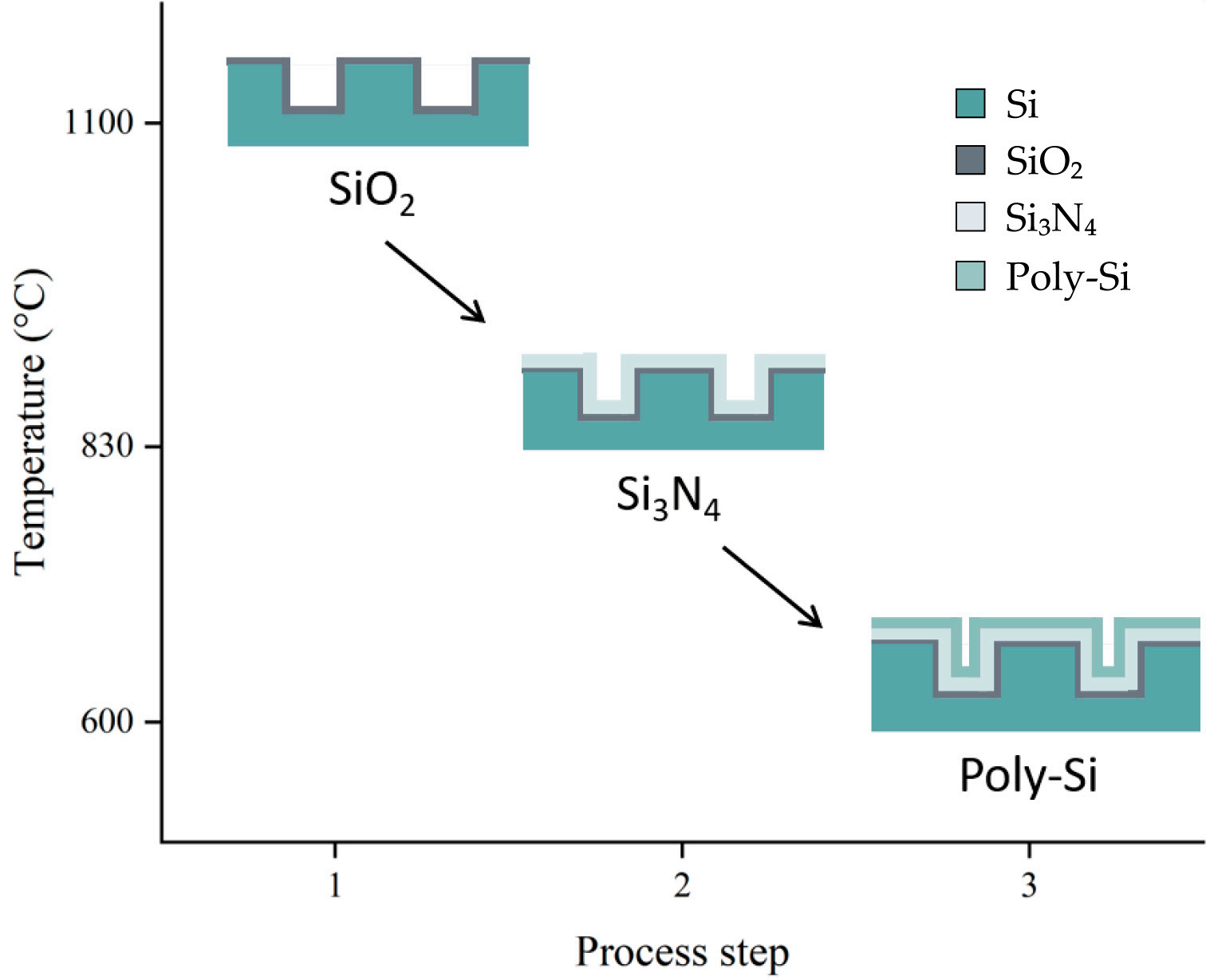
The sample tested was manufactured using silicon (Si) wafers 150 mm in diameter with a thickness of 725 µm. After an initial cleaning, a hexagonal grid composed of circular openings with diameters of 6 µm and a distance of 3 µm between the nearest neighbors was patterned with lithography. The vias were etched to a depth of 30 µm. Then, a silicon dioxide (SiO2) dielectric layer 0.3 µm in thickness was formed by dry thermal oxidation at a temperature of 1100 ◦C. Next, a 1.6 µm-thick layer of silicon nitride (Si3N4) was deposited by LPCVD (low pressure chemical vapor deposition) at a temperature of 830 ◦C. The top electrode was formed by the deposition of in situ n+-doped polysilicon (poly-Si) using LPCVD with a 0.5 µm thickness at 600 ◦C. The simplified schematic of the manufacturing process is illustrated in Figure 1. It is worth noting that these layers are deposited at varyingtemperatures, leading to misfit strain at room temperature due to their differentCTE, asreferenced in [18-21].

Figure 1. Simplified schematic of manufacturing process. Si substrate, SiO, layer deposition at1100 “C; Si₃N4 layer deposition at 830 °C; Poly-Si layer deposition at 600 °C.
The silicon substrate used in this paper has a diameter of 150 mm and a thickness of725 um. As seen in Figure 2c, the vias have a diameter of 6 um, a depth of 30 um, anda distance of 3 um between them. The layer thicknesses of SiO2, SiN4, and poly-Si are0.3 um,1.6 um, and 0.5 um,respectively.

Figure 2. The extraction process and the dimensions of the RVE. (a) Side view of the wafer; (b) Sideview of the via layer, (c) Representation of the RVE structure.
2.2. Multi-Scale Analysis for Thermal and Mechanical Properties
Due to the large number of small vias on the wafer, simulating the full geometry model directly is computationally costly. Therefore, it is imperative to adopt a multi-scale method. The initial stage of the multi-scale method involves extracting an RVE from the via layer. The extraction process and the dimensions of the RVE are illustrated in Figure 2. Overall, the multi-scale method comprises two scales of simulations. In the meso-scale simulation, the effective properties of the RVE are determined by using a homogenization method. In the macro-scale simulation, wafer warpage results are calculated by applying the effective properties of the RVE to the via layer. During the deposition process, the dielectric layers will stack on the back side of the substrate simultaneously. These backside layers are modeled as surface coatings in the simulation. However, due to their small thickness (<3 µm) compared to the substrate (725 µm), their impact is minimal.
2.2.1. Boundary Conditions for RVE with Void Phase
In order to facilitate the creation of constraints mentioned in Section 2.2.1 in Abaqusthe RVE is initially divided into four segments. From these segments, a 1/4 RVE modelis then extracted and meshed. The void space within the RVE is filled with elastic airwhich has a zero CTE and an elastic modulus that can be ignored. Subsequently, theradial pattern" command is employed to assemble the complete RVE model, and then thehomogenization method can be applied. This process allows for easier identification ofnode pairs on opposite sides, making it easier to construct the constraints. A top view ofthe process is depicted in Figure 3.

Figure 3. A top view illustration showcasing the RVE model and its homogenization process.
2.2.3. Multi-Step Homogenization Pmcedure
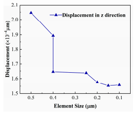
The meso-scale homogenization was preceded by a mesh convergence study a cruciastep to ensure the simulation's accuracy and efficiency. The convergence study was conducted on a 1/4 RVE model subjected to one-dimensional tensile stress. The displacemenresult in the z-direction was examined to verify mesh convergence, as shown in Figure 4 Subsequently, the homogenized properties were assessed, which revealed a relative error ofless than 1% when the mesh converged. The mesh size detemmined in this step is employedin subsequent simulations.

Figure 4. Mesh independence test by refining the mesh for the 1/4 RVE model.
3.Results and Discussions
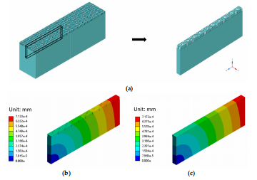
To validate the accuracy of the pmposed appmach, we created a numerical validationstructure that had ten vias, as depicted in Figure 5a. The dimensions of the vias matchedthe parameters elaborated in Section 2.1, except for a via depth of 5 um and a substratethickness of 50 um. The detailed model incorporated the materials listed in Table 1, whilethe homogenized model simplified the structure to include only Si and one homogenizedmaterial determined by the multi-step homogenization method. Identical meshing andboundary conditions were applied to the detailed and homogenized models. Both modelswere subjected to the same temperature variation of 1 °C, The simulation results of thehomogenized model and the detailed model with the actual vias were compared. As illustrated in Figure 5b c, the results showed insignificant diferences between the deformationdata of the two models, falling within a range of less than 1%. These minor differencessupported the effectiveness of our method.

Figure 5. (a) Detailed model in the numerical validation; (b) Deformation of the detailed model,(c)Deformation of the homogenized model.
4.Conclusions
This study devises and validates a multi-step homogenization method for predictingwafer warpage in silicon substrates with vias. The numerical process involves substitutingthe intricate physical prcess with a simplified temperature drop from the equivalentstress-free temperature and utilizing a homogenization method to replace the via layer witha homogenized material. Notably, the presented multi-step homogenization method differsfrom the conven tional approach by incorporating prior RVE results into the subsequentsteps. This novel method considers the influence of the previous step, thereby deliveringmore reliable results. The validity of both simplifications has been confirmed throughnumerical modeling and experimental measurements.
上一篇: 用超薄钐层钝化多晶铜