ABSTRACT: Die-to-wafer hybrid bonding is a crucial technology in advanced chiplet integration systems. Temporary die bonding on wafers and subsequent debonding are key aspects of this process. However, conventional polymer-based temporary bonding techniques involve several challenges such as issues related to the accurate placement of the die. Although direct bonding is a promising technology, such processes normally involve permanent bonds. The present study demonstrates an innovative temporary bonding method based on plasma activated direct bonding and examines the associated bonding/debonding mechanisms. In this work, a dielectric bonding film was deposited at a relatively low temperature by chemical vapor deposition. This method offers several advantages, including high alignment accuracy, limited risk of die shift, and cost reduction based on removal of the carrier wafer grinding process. Wafer bonding was performed with SiO2 films deposited at low temperatures, and voids were formed at the bonding interfaces during postbond annealing. The bonding energy was sufficiently low even after annealing to allow wafer pairs to be released as a consequence of voids serving as initiation points for debonding. Desorption gas analysis established that the SiO2 films absorbed significant moisture from ambient air, which was the root cause of void formation. Die-to-wafer bonding tests confirmed the formation of voids at the bonding interfaces. This dielectric is likely to have applications as a temporary bonding material in chiplet integration systems.
INTRODUCTION
High-performance semiconductor devices are a necessary component of systems such as artificial intelligence, cloud networks (that is, data centers), and edge devices. The concept of chiplets has received a great deal of attention as a means of reducing production costs while improving yield, power efficiency and performance.Compared with systems on a chip and so-called monolithic chip devices, chiplet integration can provide improved yields by selecting known-good die (KGD) and can also adopt dies fabricated using different technical nodes in the system. These factors can lead to cost reduction and reduce the time from research and development to the marketing stage. Furthermore, because the chiplet concept allows more design flexibility, such systems can result in increased integration density, shorter interconnections, and lower power consumption.
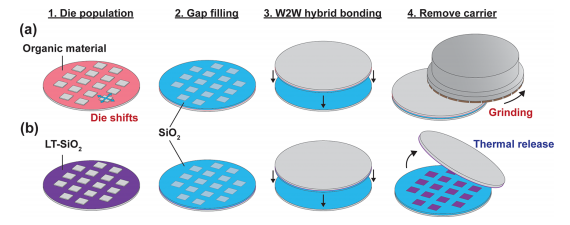
On this basis, the present work proposes a new temporary bonding method based on low-temperature-deposited SiO2 (LT-SiO2).1 The process flow during D2W bonding with LTSiO2 is summarized in Figure 1. The LT-SiO2 used in this technique is a dielectric film deposited by plasma enhanced chemical vapor deposition (PE-CVD) at a relatively low temperature of 150 °C. Temporary bonding during die placement is accomplished by direct bonding with LT-SiO2 as the bonding dielectric material (Figure 1a). This process reduces the risk of die shifts because the bonding interface is both thin and solid. Additionally, because SiO2-based direct bonding is typically used in the fabrication of such devices, this technology is compatible with most front-end processes. As noted, D2W bonding tools have not yet matured, but a small degree of bonding failure can be accepted in the case of temporary bonding. Furthermore, LT-SiO2 forms voids at the bonding interface during annealing that allow the carrier wafer to later be removed using a thermal release technique (Figure 1b).

Figure 1. D2W integration processes using (a) an organic material and (b) LT-SiO2 as the temporary bonding interface.
EXPERIMENTAL SECTION
A number of p-type 200 mm Si(100) wafers were employed for the W2W bonding trials. A 150 nm LT-SiO2 layer was deposited on each wafer by PE-CVD at 150 °C, using liquid tetraethyl orthosilicate (TEOS) mixed with gaseous O2 as precursors, at a deposition pressure of 50 Pa and radio frequency power of 1000 W. Following deposition, the dielectric surface was planarized using an ACuPLANE LK393C4 slurry. Following this, a 50 nm portion of the LT-SiO2 layer was removed by chemical and mechanical polishing, leaving a 100 nm-thick layer. Each specimen was subsequently subjected to postdeposition annealing (PDA) under N2 at different temperatures. The wafer pairs were then activated by exposure to a N2 plasma for 60 s, after which the wafer surfaces were rinsed with deionized water. Wafer bonding was performed at room temperature in clean ambient air. The initial contact was carried out while applying a low pressure at the center of the wafer pairs, after which postbond annealing (PBA) was performed.
In contrast, D2W bonding experiments were performed using ptype 300 mm Si(100) wafers. Exactly the same process was applied to the 300 mm wafers as had been employed with the 200 mm wafers up to the PDA step. At this point, the backside of the top wafer was thinned to 200 μm. After grinding, the wafer was singulated into dies with a size of 10 × 10 mm.11 Following this, the wafer surface was cleaned and activated using the same process as that applied during the W2W bonding. After wet cleaning, die bonding was performed using a particle-less, noncontact-type D2W bonder.
Figure 2 presents AFM images of the LT-SiO2 surfaces. The root-mean-square surface roughness values for this material after CMP, exposure to a 100 W N2 plasma, and exposure to a 250 W N2 plasma were 0.15, 0.21, and 0.85 nm, respectively. The CMP process evidently generated atomic-level flatness on the LT-SiO2 surface (Figure 2a). Although this smooth surface was maintained after treatment with 100 W plasma (Figure 2b), some defects were formed after treatment with 250 W plasma (Figure 2c). It should be noted that 250 W is not an overly high power setting for plasma activation. The LT-SiO2 was evidently more sensitive to ion bombardment than the thermal SiO2 because of the minimal mesoscopic structure of the former, which caused surface etching and redeposition, leading to defect formation.

Figure 2. AFM images of LT-SiO2 specimens (a) after CMP, (b) after exposure to 100 W N2 plasma, and (c) after exposure to 250 W N2 plasma.
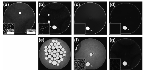
To investigate the effect of the plasma power and PDA temperature on the void formation, LT-SiO2 pairs were bonded and annealed. Figure 3 provides SAM images of the bonding interfaces. In the present article, voids less than 1 mm are defined as microvoids. Immediately after bonding, microvoids were observed only in those pairs made with the higher plasma power of 250 W (Figure 3a). In the case of the bonding pair made using this high plasma power, the microvoids might have been caused by the rough surface (that is, by the presence of micro defects) that limited the contact area between the wafers. The other three pairs were bonded without voids, except for those caused by particles. In the present work, void formation was not undesirable because the goal was to use LT-SiO2 as a temporary bonding material, and hence the voids served to initiate debonding. However, since wafers must be firmly bonded so that they can withstand subsequent processing until the carrier wafer is removed, void formation immediately after bonding should be avoided. Therefore, plasma activation at 100 W was selected as optimal. It should also be noted that large voids appeared in the wafer pair fabricated without PDA after PBA at 150 °C (Figure 3e). In addition, microvoids were also observed in the case of the pair subjected to PDA at 150 °C while only a few voids were observed on the pair made with PDA at 250 °C.

Figure 3. SAM images of LT-SiO2 specimens (a−d) after bonding and (e,f) after PBA at 150 °C. These treatments were performed (a) with high plasma power, (b,e) without PDA, (c,f) with PDA at 150 °C, and (d,g) with PDA at 250 °C.
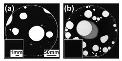
Bonding pairs fabricated with PDA at 150 and 250 °C were also subjected to PBA at 250 °C. As shown in Figure 4, both pairs exhibited very large voids, suggesting that voids were produced when the PBA temperature was equal to or above the deposition temperature of 150 °C or the PDA temperature.

Figure 4. SAM images of LT-SiO2 specimens after PBA at 250 °C and with PDA at (a) 150 or (b) 250 °C.
CONCLUSIONS
This work demonstrated temporary direct bonding with LTSiO2 and investigated the characteristics of the resulting films with regard to D2W integration. Voids were formed at the bonding interface during W2W bonding trials in the case in which the PBA temperature exceeded the deposition or PDA temperature. Hence, the bonding energy was sufficiently low to make debonding possible. The TDS results established that the LT-SiO2 absorbed water from the air but also desorbed a significant quantity of water even after annealing, leading to void formation. The PAS results also suggested that water evaporated from these films, such that open spaces were formed during annealing. Voids were also generated during D2W bonding after annealing as well as during W2W bonding. It is apparent that LT-SiO2 can be used as a temporary direct bonding interface material in D2W integration.
上一篇: 用于硅片翘曲估计的多步机械和热均质化
下一篇: 马兰戈尼干燥模型