Abstract: In this work, we demonstrate photonic fabrication by integrating waveguide resonators and groove structures using cost-effective i-line stepper lithography on a 6-inch full wafer. Lowloss silicon nitride (SiN) waveguide can be realized with the quality (Q) factor of waveguide resonators up to 105 . In addition, groove structures are also integrated by the full-wafer process, providing long-term stability of coupling and package solutions. The uniformity of different die locations is verified within the full wafer, showing the good quality of the fabricated photonic devices. This process integration of photonic devices provides the potential for mass-productive, high-yield, and high-uniformity manufacturing.
1. Introduction
With the advancement of science and technology, precision manufacturing and micro/nano fabrication now play an important role in meeting the world’s evolving demands, particularly in applications of high-speed computing, communication, and transportation. The development of electronics and network systems over the past century has brought an evolution to in modern society. Owing to the burgeoning development of complementary metal-oxide-semiconductor (CMOS) manufacturing technology, digital devices based on integrated circuits (IC) have widely spread, becoming an integral part of our daily lives. Nowadays, this fabrication platform is continuously developed to enable the realization of integrated photonics over the past few decades. By utilizing optical signals as the carriers, photonic devices have been discussed in the realms of optical communications, optical sensing and ranging, integrated light sources and optoelectronic systems, artificial intelligence and neural networks, and quantum and nonlinear photonics. Despite extensive research efforts, most of the photonic applications still remain primarily as benchtop models in the laboratory, mainly due to the fabrication challenges and absence of standardized processes. Besides, the pursuit of large-scale, mass-production fabrication techniques for integrated photonics remains relatively unexplored, and most of the demonstrations are still in the prototype stage. In this work, we demonstrated the integration of silicon nitride (SiN) waveguide resonators and groove structures by i-line (365 nm) stepper lithography on a 6-inch wafer. Among all the photonic devices, waveguide microresonators have gained intensive attention due to their widespread applications within integrated photonic circuits, serving various optical functions like modulators, filters, detectors, and nonlinear signal generators. By implementing waveguides as the photonic platform, ultra-low-loss waveguides and resonators with high quality (Q) factors have been successfully demonstrated. However, these studies are achieved either through a 4-inch wafer (100 mm diameter) technology or spliced devices or require time-consuming electron-beam / costly deep ultraviolet (DUV) lithography processes. A few recent studies show the potential to fabricate ultra-low-loss waveguide resonators within a full-wafer technology; however, DUV lithography is still required; or the resolution is limited by the contact lithography. Besides, no other layers are further integrated. In the meantime, the nanoimprinting method has been introduced for fabricating 6-inch photonic devices, but it only shows single-layer patterning. Our work has yielded several new findings. First, we show the capability to integrate photonics devices, including both waveguide resonators and groove structures onto a 6-inch full-wafer process. Second, a low-loss SiN waveguide is realized with the Q factor of resonators up to 105 using cost-effective i-line stepper lithography in a full-wafer integrated process. Third, full-wafer groove structures for fiber-to-integrated waveguide coupling are also fabricated, providing better coupling stability at a high input power. Last, the high uniformity of the fabricated devices from edge to center is verified. These demonstrations pave the way to future integration of SiN-based photonics with a foundry-standard fabrication process.
2. Waveguide and resonator design
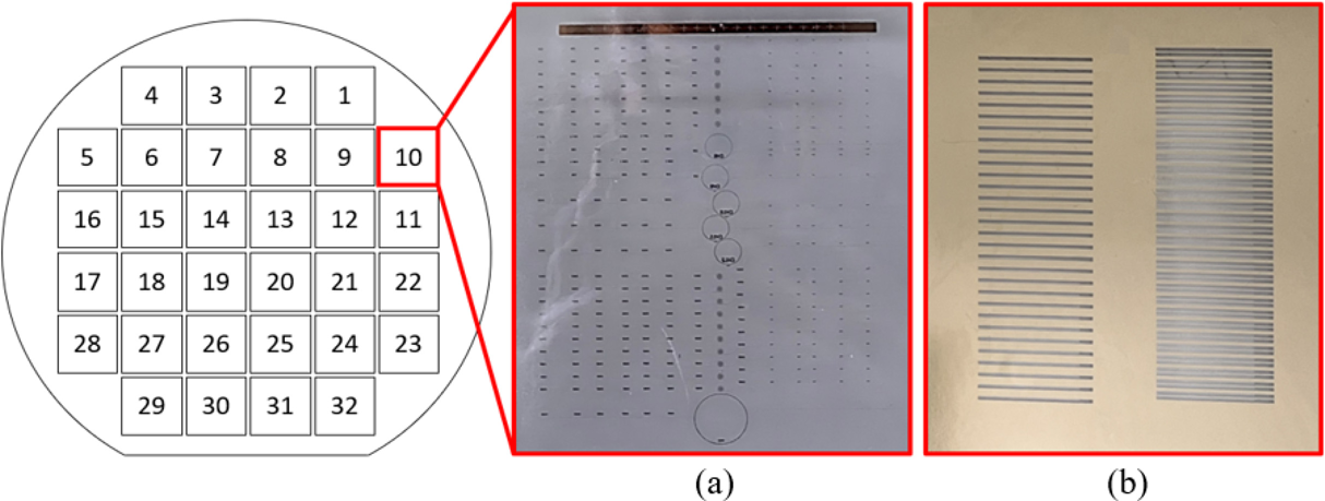
To implement photonic integration onto 6-inch full wafer, two distinct masks are designed to realize the SiN photonic waveguides and U-groove structures. Figure 1(a) and 1(b) show the mask images of waveguide resonators and the U-groove structures, respectively.

Fig. 1. Mask images of (a) waveguide resonators and (b) groove structures.
The first mask is used to define the waveguide pattern, including the bus-waveguides, waveguide resonators, and tapers for efficient edge-coupling. The waveguide width of the bus and resonators is set at 1 µm and 3 µm, respectively. The bus-waveguide is aimed to support single-mode propagation, while the resonator-waveguide allows multi-mode propagation for loss minimization. The gap size between the bus and resonator-waveguide is designed at 0.4 µm to accommodate the resolution limit of the i-line stepper (> 350 nm); the small gap helps to improve the coupling efficiency and enhance the extinction ratio of waveguide resonators. The edge of the bus-waveguide is also tapered down to 0.4 µm to mode-match with the coupled fibers. For the second reticle, groove structures are patterned corresponding to each channel. It is worth noting that, by the layout design, the waveguide edge is self-aligned to the groove structures, obviating the need for complex dicing and polishing. It also provides better coupling uniformity. The exemplary schemes for waveguides with an edge-taper and grooves are shown in Fig. 2(a) and 2(b).

Fig. 2. Schematic diagrams of (a) waveguides with an edge-taper and (b) waveguides with groove structures.
3. Device fabrication
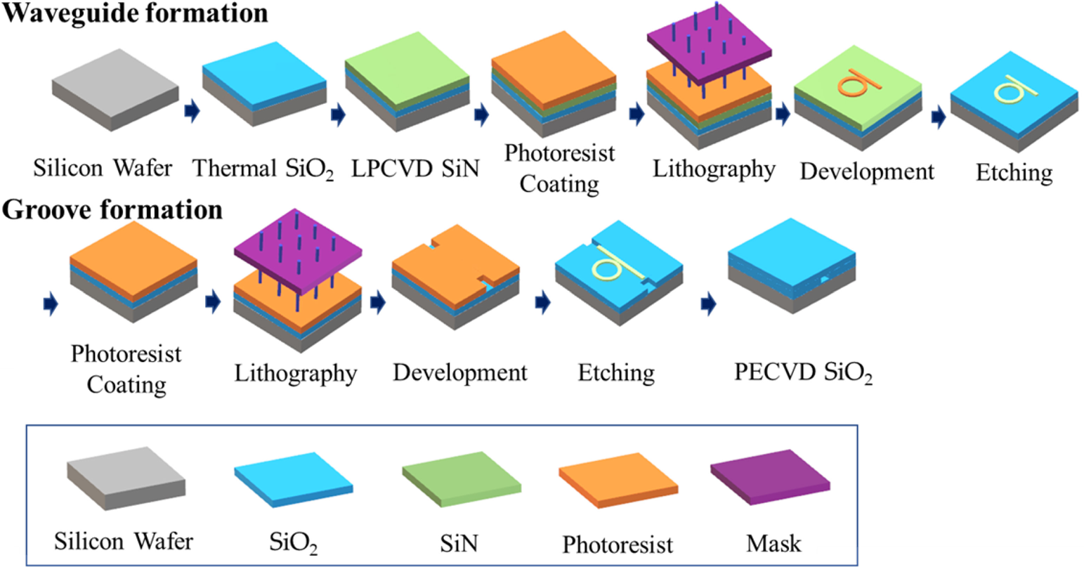
The fabrication process is illustrated in Fig. 3. First, a 2 µm thick silicon oxide (SiO2) layer is thermally grown on a 6-inch silicon wafer in a diffusion furnace. A 500-nm SiN film was then deposited as a core layer by low-pressure chemical vapor deposition (LPCVD) at 800°C, providing a highly-confined waveguide core with negligible stress-induced cracks. No significant crack is identified under the growing conditions of a low-stress SiN layer. To adapt the foundry-standard fabrication process, three lithography steps of i-line steppers are used to configure the patterns, as shown in Table 1. We discuss the fabrication processes in detail as follows.

Fig. 3. Schematic diagram of the process flow.
3.1. 1st step for establishing alignment markers
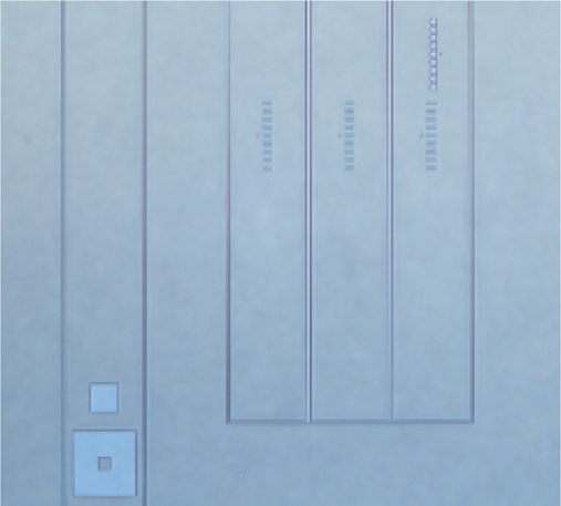
To define the position for the subsequent patterning, we first pattern the alignment markers using the i-line stepper (FPA-3000 i5+) with a 750 nm thick positive tone photoresist (PFI38) at a dosage of 1325 J/m2 We should note that the zero layer of the alignments is defined on a different reticle in the i-line stepper by default and is exposed by the multilayer program in the stepper. In comparison to the previous work where the alignment markers are fabricated by the stepper and later used for the alignment of a spliced device in the contact lithography, the alignment markers are defined at each die through the full wafer. Then, CF4-based etchant in a polycrystalline silicon dry etcher (TCP9400) is used to transfer the alignment patterns onto the SiN film. The etching depth of the alignment markers is 332 nm at an etching rate ≈ 1.76 nm/s. The developed alignment markers are shown in Fig. 4.

Fig. 4. Alignment marker after development.
3.2. 2nd step for fabricating SiN-integrated waveguides
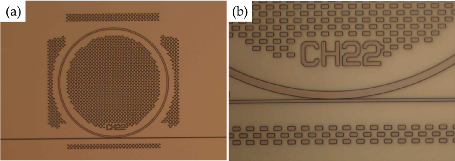
Subsequently, we pattern the photonic waveguide by again using the same lithography and etching processes. The etching process is set at 300 s to ensure a fully-etched SiN waveguide with a height of 500 nm. Figures 5 show the fabricated waveguide resonators, and dummy patterns around the waveguide are used to alleviate the pattern loading of the etching process.

Fig. 5. (a) Microscope images of the fabricated waveguide resonators and (b) the corresponding zoom-in image.
4. Discussion
To compare with the previous studies in SiN photonic waveguides, we show the comparison of different fabrication schemes in Table 2. This work here realizes high-Q SiN waveguide resonators onto 6-inch full wafers with the cost-effective, sub-µm resolution proximity i-line stepper lithography. We should note that the relatively lower Q factors from our demonstration are due to the only 2 µm buried SiO2 layer and no furnace annealing to the SiN film for the full-wafer processes. Typically, a thick buried SiO2 layer or thermal annealing of SiN film is required for the improvement of Q factors . These requirements can be easily met upon transitioning to commercial production within a well-established foundry. To clarify these issues, we have fabricated another spliced device using the same i-line stepper process with a SiN film onto a 4 µm thermal SiO2 layer, followed by an additional 1050 °C annealing for 12 hours. The Q factors can then be achieved up to 1.2 × 10⁶ . In comparison with the widely, commercially used DUV lithography, the i-line stepper has lower costs on equipment, ownership, and resists, showing an attractive option in realizing photonic devices with compromised resolution and decent quality. Furthermore, the resist of i-line steppers shows negligible shrinkage during photostabilization, while DUV resists typically have higher resist shrinkage as high as 25%, which causes the change in patterning and the critical dimensions. In addition, the groove structures are also integrated into the 6-inch full wafer to enhance the coupling stability. This demonstration shows the potential for future photonic integration with large-scale manufacturing and foundry-ready CMOS processes.
5. Conclusion
In summary, we demonstrated photonic waveguides based on the SiN platform in a 6-inch full wafer. The Q factor can be up to 105 while the within-die variation is 9% at the center and 13% at the corner. Stable coupling can be achieved at high powers, even up to 300 mW, by integrating the full-wafer groove structures with the aid of the i-line stepper lithography. This work realizes the potential for photonic integration with foundry-ready, CMOS-compatible manufacturing.