Abstract— SiC power MOSFETs with trench-gate structure have been irradiated with heavy-ion broad-beam and microbeam. Microdose effects resulting in higher subthreshold drain leakage were observed when irradiating the devices at low drain-source voltages and reported for the first time for SiC power devices. Increasing the drainsource bias during the exposure, single-event leakage current (SELC), characterized by microbreaks in the gate oxide was measured. The accumulation of microbreaks eventually led to a complete gate rupture. The differences with respect to the SiC planar-gate MOSFETs and the impact of these results on the testing procedures for the two technologies are discussed.
I. INTRODUCTION
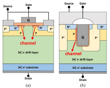
Silicon Carbide (SiC) power MOSFETs have gained significant attention in recent years due to their unique properties and advantages over traditional silicon-based MOSFETs. SiC power devices are capable to withstand higher internal critical fields than their silicon counterparts, making them ideal for high-power applications such as electric vehicles, renewable energy systems, and industrial equipment. They are also known for their low on-resistance and high switching speeds, which results in lower power consumption in the semiconductors and leads to overall higher energy conversion efficiency. SiC power MOSFETs are commercially available in two gate designs: planar and trench. While both designs are based on the same fundamental principles of operation, they differ in their physical structure and performance characteristics. Planar gate SiC power MOSFETs have a surface horizontal channel; this design is simpler to manufacture and has widely been used in the industry for many years. On the other hand, in the trench-gate architecture the gate is etched into the silicon carbide epitaxial layer, the channel is vertical and the JFET resistive region is avoided, leading to superior on-state performance. However, the trench-gate architecture is more complex to manufacture and can be more expensive than their planar counterparts. Nowadays symmetric and asymmetric trench designs are available on the market.Fig. 1 shows the schematic layouts for a SiC planar-gate MOSFET and an asymmetric-trench MOSFET.

Fig. 1. Schematics layouts for (a) SiC planar-gate MOSFET and (b) SiC asymmetric-trench MOSFET.
SiC power devices are also becoming increasingly popular in the field of space exploration. The possibility to operate SiC devices at high voltage, current, and temperature, and the ability to switch at comparably high frequencies with reduced losses would greatly improve the overall electrical efficiency of onboard systems, resulting in a more compact design, lower weight, and enormous cost saving. For example, due to the capability of SiC to operate at temperatures higher than 460˚C, SiC integrated circuits are currently considered for Venus surface exploration missions. However, despite the beneficial characteristics, the adoption on SiC power devices in space is still limited due to the sensitivity to radiation, which increases the risk of single event effects (SEEs). Galactic cosmic rays (GCRs) represent the higher risk in space, as they are composed of energetic heavy ions that can pass practically unimpeded through a typical spacecraft, inducing SEEs.
Depending on the linear energy transfer (LET) of the ion and on the bias conditions (i.e., drain-source and gate-source voltages) during the exposure, different types of SEEs have been observed in SiC power MOSFETs. When irradiating the device in OFF-state and at low drain-source voltages (VDS) during the exposure, higher drain current (ID) is observed due to the ionization generated by the impinging particle. This effect is called charge collection and it is non-destructive. Partial degradation such as single event leakage current (SELC) is observed at higher VDS, characterized by permanent increase of gate (IG) and drain leakage currents with increasing heavy-ion fluence. After the exposure, the device is still operational, but its characteristics are exceeding the specification limits due to the increased leakage current. Previous works reported two different mechanisms for SELC; initially, microbreaks are formed in the gate oxide, inducing a drain-gate leakage path, as previously reported for Si power MOSFETs. At higher voltages, a second mechanism is observed, characterized by higher increase of the ID with respect to the IG, which has been associated with the creation of extended defects in the device (i.e., different types of stacking faults). Finally, at higher VDS during the exposure, complete and irreversible loss of the electronic component due to catastrophic failure such as Single Event Burnout (SEB) and Single Event Gate Rupture (SEGR) are observed.
II. EXPERIMENTAL METHOD
Two experiments were performed with broad-beam: one at the Heavy-Ion Facility (HIF) of the Université Catholique de Louvain, Louvain-la-Neuve, Belgium and the other at the RADiation Effects Facility (RADEF) in the Accelerator Laboratory of the University of Jyväskylä, Finland. Different ion species were selected for the irradiations, as reported in Table I. Yet another experiment was carried out using a microbeam at the UNIversal Linear ACcelerator (UNILAC) micro-probe line at the Helmholtzzentrum für Schwerionenforschung (GSI) in Darmstadt, Germany. The main difference among these experiments are the beam characteristics, as reported in Table I and Table II. The broad beams used at HIF and RADEF delivered a wide and uniform beam of radiation with a diameter of 2.5 cm at HIF and squared beam of 2×2 cm2 at RADEF. In contrast, the microbeam used at UNILAC provided a beam with a focal spot of 500 nm to target micrometric areas selected with an optical light microscope situated in the chamber. To ensure the irradiation with a preset number of particles and to avoid double hits at the same position, a fast electrostatic beam switch is controlled by the hit detection system for the microbeam irradiation. When a hit is detected, the microbeam is switched off and the focal point of the probe is moved to the new x-y coordinates.
Fig 2 (b) illustrates a second mechanism of damage induced by the ions when the VDS during the irradiation is set over a second threshold (i.e., VDS = 120 V for Kr). Steps in the ID and IG are observed during the exposure, indicating the formation of microbreaks in the gate region. In addition to what is described in Fig. 2 (a), an increase of IG is also observed in the transfer and in the blocking characteristics in the central and right panels. For the latter, a gate-drain leakage path is observed for the current for VDS > 600 V. This mechanism can be explained as SELC degradation, as previously reported for SiC planar devices in [14] and associated with the formation of microbreaks in the gate oxide. However, in contrast to results observed for the planar architecture where the ID and IG increase with the same rate and in absolute values, a higher ID leakage is observed for the trench-gate architecture due to the microdose effect in sub-threshold, which increases with increasing total fluence.

Fig. 2. (a)
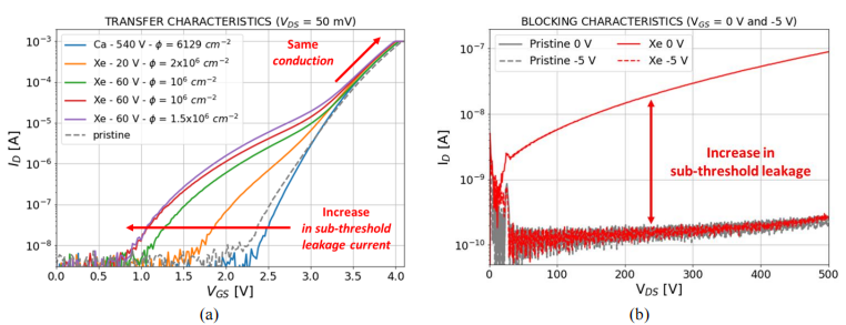
After the exposure, additional measurements were performed on all the samples showing microdose degradation (ID increase in sub-threshold). Fig. 3 (a) shows the transfer characteristics for five devices irradiated in different conditions. Increased leakage through the channel is observed in the sub-threshold region. However, no effect on conduction and no rigid shift of the threshold voltage is observed, such as in the case of X-rays irradiations. The channel resistance (Rch) of the component is moderately decreased, showing an impact in sub-threshold, where it has a larger contribution on the total RDS(ON). A dependency on the LET, the bias applied during the exposure and the total fluence is observed. In Fig. 3 (b) the blocking characteristics measured at VGS = 0 V and VGS = -5 V is reported for a device irradiated with Xe at VDS = 60 V and a fluence of 106 ions/cm2 . Increased drain leakage is measured when performing the sweep at VGS = 0 V. However, when repeating the measurement applying VGS =-5 V, the leakage drain current is reduced and remains comparable to pristine levels. These results indicate that the increase observed in the first measurement is caused by the degradation of the subthreshold channel leakage current, and not by the creation of extended defects as previously reported for SiC planar-gate MOSFETs characterized by higher ID increase during the exposure .

Fig. 3. Post-irradiation analysis of SiC trench power MOSFETs degraded in the first region (ID increase). (a) Transfer characteristics measured at VDS = 50 mV, (b) Blocking characteristics measured at VGS = 0 V and -5 V for a pristine sample and a sample irradiated with Xe at VDS=60 V and ɸ = 106 𝑐𝑚−2 .
Ⅲ. CONCLUSIONS
Prototype SiC power MOSFETs with a trench architecture were tested with heavy ions using broad-beam and microbeam irradiations. In all the devices under test, microdose effects resulting in higher sub-threshold drain leakage were observed and associated with the creation of localized parasitic transistors with lowered threshold voltage, as reported in literature for Si technologies. Such effect strongly depends on the angle of incidence of the primary ion and can have an impact on the testing procedures.
Single event leakage current characterized by the formation of microbreaks in the gate oxide was observed at higher voltages and led to a complete gate rupture. At the voltages selected for the test, none of the devices showed SEB nor the typical signature of damage observed in SiC planar gate MOSFETs characterized by higher degradation of the drain current (i.e., SELC II). Overall, it has been shown that under heavy-ion irradiation, similar to Si technology, gate oxide damage is the primary cause of failure in SiC trench devices.
The impact of these results on the testing procedures were discussed, highlighting the differences between planar and trench SiC MOSFET technologies, with special attention on the angle of incidence, the flux and the accumulated fluence.