Abstract—Silicon ring resonators on SOI substrates are well known and widely studied. They are commonly used in datacom and high-performance computing for wavelength multiplexing and spectral filters. They can be tuned to the desired frequency with resistive heaters, which is the primary power budget of the device. In this work, the impact of backside cavities etched in the bulk silicon of SOI substrates below ring resonators is studied. Simulations show that those backside cavities improve significantly heat confinement and minimizes heat losses usually due to conduction in the Si substrate. Backside cavities have been successfully etched in the bulk of the SOI substrate to improve heat trapping within the silicon rings. The etching process is compatible with the standard silicon photonics interposer process flow.
Power consumption studies have been performed with a reference ring resonator on SOI and ring resonators with different backside cavity diameters. These results will be discussed with respect to the backside cavity opening. A 72% power consumption reduction for a 10 µm diameter ring resonator on SOI has been achieved with a backside opening of 100 µm deep and 40µm diameter. The cavities opening did not impact the optical ring performances.
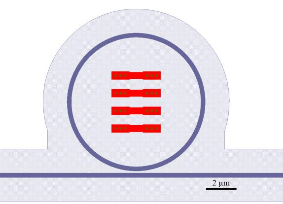
Figure 1: Scheamtic view of the ring resonator (purple) and the silicon heaters (red)
I. INTRODUCTION
Silicon photonics propose an interesting path for increasing bandwidths for high speed communications in datacenter and high-performance computing applications. This technology can leverage the technical know-how of traditional CMOS foundries to make performant and reliable systems. A common optical solution in the field of silicon photonics is to use wavelength multiplexing to increase bandwidths of transceivers and optical networks on chips (ONoC) communication. In this framework, multiple wavelengths of infrared light are injected in a single waveguide. The multiple wavelengths are then demultiplexed at the point of use, thanks to a spectral filter, such as a ring resonator (RR).
II. FEM SIMULATION
In this part, the effect of a cavity on the backside of the substrate is studied. A 3D model of a RR with appropriate dimensions id created using COMSOL software. A power density is applied at the center of the ring such that the temperature inside the ring reached 100°C. This is repeated with three different cavity diameters: 25, 30 and 40 µm. For each cavity diameter, the power density is adjusted to match the temperature of 100°C in the ring. This power density is finally converted to power by multiplying the power density by the volume of the heater element.
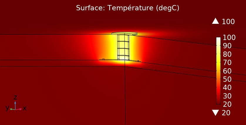
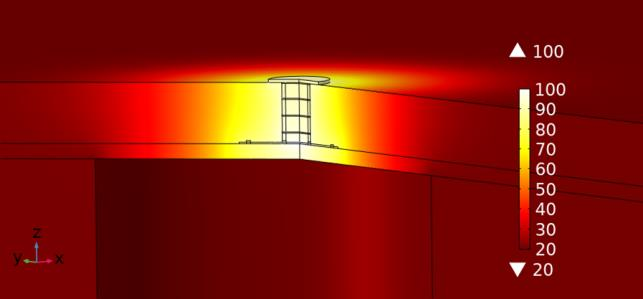
As shown on figure N, the presence of the cavity changes the temperature field. The temperature is more uniform in the ring region. The heat also diffuses farther away from the ring, as illustrated in figure X, which shows the temperature along the ring radius. The temperature in the case of a ring without a backside cavity (in black) reaches equilibrium at 10 µm from the center (i.e. 2 radii), while backside cavities increase this distance up to 25 µm, or 5 radii. In most real-world designs, the rings are spaced out by more than 25 µm, therefore the thermal cross talk between adjacent rings can be neglected.
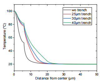
Figure 2: Temperature profile along a ring radius
III. PROCESS
This work is based on STMicroelectronics 2nd generation Siphotonics process, using 300 mm SOI wafers with 1.5 µm buried oxide layer (BOX) . The silicon RR of interest have a 10 µm diameter with heaters of doped silicon on the waveguide level, in the middle of the resonator. The heater module is composed of 4 strips of doped Si located on the waveguide level, as shown in the middle of the ring of Figure 3, with 4 rows of 2 rectangular marks. By supplying them a direct current, these resistors will heat up thanks to Joule effect, increasing the temperature in their vicinity. The waveguides used in our rings are in deep-rib configuration with a 50 nm slab. The rings are connected thanks to four metal levels and Al pads for testing. A schematic cross section of the wafer can be seen in Figure 4.

Figure 3: Optical top view of microring (purple and yellow) and etched cavities footprint to scale (green – 25 µm, red – 30 µm and blue – 40 µm)
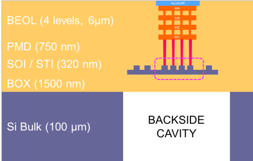
Figure 4: Schematic cross section of the stack at the end of process (not to scale)
After this standard photonic process (Figure 5 a), the front side of the wafers are bonded on carrier wafers with temporary glue (Figure 5 b), and thinned down to 100 µm. This thickness is compatible with the height of TSV-Mid process (10×100 µm) that will be integrated in similar wafers in order to create photonic interposers. The cavity patterning alignment is done on front side with Metal 1 marks thanks to a dedicated infrared Canon stepper. Marks have been chosen at Metal 1 level to insure a strong infrared contrast through the thinned silicon substrate from the wafer backside. Our alignment approach grants an accuracy below 1 µm between the waveguide level and the backside cavity. An 8 µm thick TCIR photoresist has been selected for the backside cavity lithography thanks to high etching selectivity with Si.
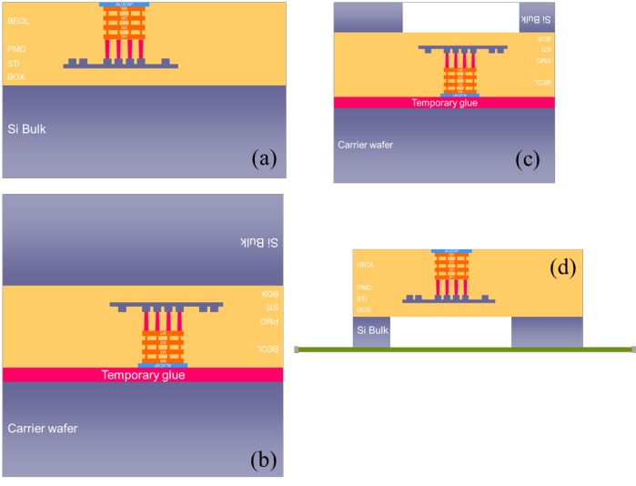
Figure 5: Process flow of the backside cavity
After the backside etching (Figure 5 c), the thin wafer is debonded from its temporary carrier using an EVG820 tool to a handling tape and frame compatible with the prober station (Figure 5 d). In the case of TSV-mid process integration for photonic interposers , processed wafers could follow the standard backside process route (BRDL, organic passivation and under ball metallization). However, in this study no TSVs are implemented in the tested wafers.
V. RESULTS AND DISCUSSION
The impact of the cavities is deduced by comparing the tuning powers of the rings with different cavity diameters to a reference ring without cavity. Table 2 summarizes the average tuning power and their standard deviation for the different cavities and for the reference ring, as well as the relative improvement of the cavity on the tuning power compared to the reference ring.
VI. CONCLUSION
In this work, backside cavities have been successfully processed on silicon photonics wafers and evaluated. The developed process flow exhibits no incompatibly with a standard silicon photonics interposer process flow. These cavities allow to significantly lower power consumption for thermal tuning without undesirable changes in the ring behavior. It is shown that a 100 µm deep, 25 µm diameter cavity on a 10 µm ring reduces the tuning power needed by 67%, without changing the behavior of the ring, while a 40 µm cavity reduces the tuning power by 72%.
The Si/SiO2 selectivity of the etching process allows multiple cavity diameters to be etched in a single step, allowing flexibility in the design of the photonic front end and minimal engineering for the realization of the backside cavity.
The cavities also introduce a longer cooling time, reducing thermal switching frequencies and must be taken into consideration for some applications.
上一篇: 马兰戈尼干燥模型