Abstract. This work gives an overview on different technological solutions for polysilicon removal in industrial tunnel oxide passivated contact (i-TOPCon) n-type silicon solar cell fabrication. The removal of parasitically deposited poly-Si layers on the front and the edges is a mandatory requirement for a low reverse bias junction leakage current (Irev). A polysilicon removal study on wafer level shows (i) that the efficient removal of the surface oxide layer before poly-Si etching is crucial to achieve short etching times and (ii) that an additive in the KOH solution enhances etching selectivity between poly-Si and silicon oxide surfaces. To evaluate the impact on device level, TOPCon cells have been fabricated in parallel using in-situ n-doped PECVD and LPCVD layers, as well as ex-situ LPCVD poly-Si layers, with another variation of poly-Si removal processes, namely wet chemical inline, wet chemical batch cluster and atmospheric dry etching (ADE). Our results show that a two-minute inline polysilicon removal in hot KOH meets the Irev qualification in case of as deposited in-situ doped layers, whereas for ex-situ doped layers a batch process with a five-minute KOH etching time is needed. LPCVD poly-Si cells show efficiencies above 23%, PECVD poly-Si cells with a batch cluster poly-Si removal process up to 23.4%.
1 Introduction
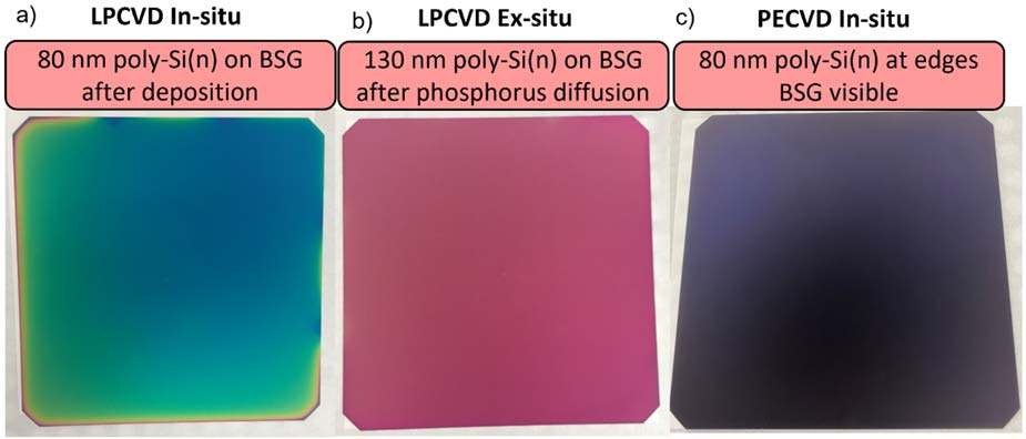
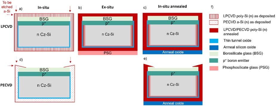
Industrial tunnel oxide passivated contact (i-TOPCon) solar cells are in focus of photovoltaics (PV) industry and research. The deposition of the poly-Si layer on the rear side is a key aspect for TOPCon solar cells. The TOPCon layer stack (tunnel oxide and doped poly-Si) that is needed for carrier selectivity is usually deposited by low pressure chemical vapor deposition (LPCVD), or plasma enhanced chemical vapor deposition (PECVD). LPCVD n-doped poly-Si layers are currently still mainstream in industry, typically combined with ex-situ doping, i.e. n-type doping of an intrinsic Si layer in a following POCl3 diffusion process. The ITRPV 2022 roadmap suggests that transition from LPCVD to PECVD poly-Si deposition will take place in the upcoming years. The doping of the PECVD TOPCon layers is usually done in-situ, i.e. during deposition, because for this technology the deposition rate for in-situ doping is as high as for intrinsic poly-Si. At Fraunhofer ISE, the industrial route of TOPCon technology was based on in-situ phosphorus doped LPCVD layers.All the deposition processes, either LPCVD with loading one wafer per slot or alternatively front-to-front loading or PECVD with a target single side deposition, lead to some wrap-around and therefore a parasitical poly-Si deposition on the front side and the edges. For LPVCD the wraparound to the front side of the solar cellis complete (one wafer per slot), for PECVD only at the edges (Fig.1).

Fig1
In this article we focus on wet chemical removal of the parasitical poly-Si in hot diluted potassium hydroxide (KOH) because it is highly relevant for industrial TOPCon cells for reasons of cost efficiency and availability of chemicals in existing production lines. Single side wet chemical etching using KOH has been established successfully to remove the parasitic boron emitter (chemical etch isolation, CEI) on the rear side of TOPCon solar cells. This knowledge can be transferred to poly-Si removal. In general, the single side wet chemical polysilicon removal can be realized as an inline process or as a batch cluster process. An inline process is a roller based single side etching process with direct contact of the wafers to the transport rollers. In a batch processing tool, wafers are immersed as a whole unit, which highlights the need for a rear side protection layer. This layer has been usually phosphosilicate glass (PSG) that was formed during POCl3 doping for the LPCVD ex-situ route (Fig. 2b). PECVD poly-Si is usually doped in-situ and therefore does not feature any dielectric protection layer (Fig. 2d). The idea is, to realize a batch removal of in-situ doped poly-Si without an additional process step using the anneal oxide that is formed in a thermal anneal process (Figs. 2c and 2e).

Fig2
2 Experimental
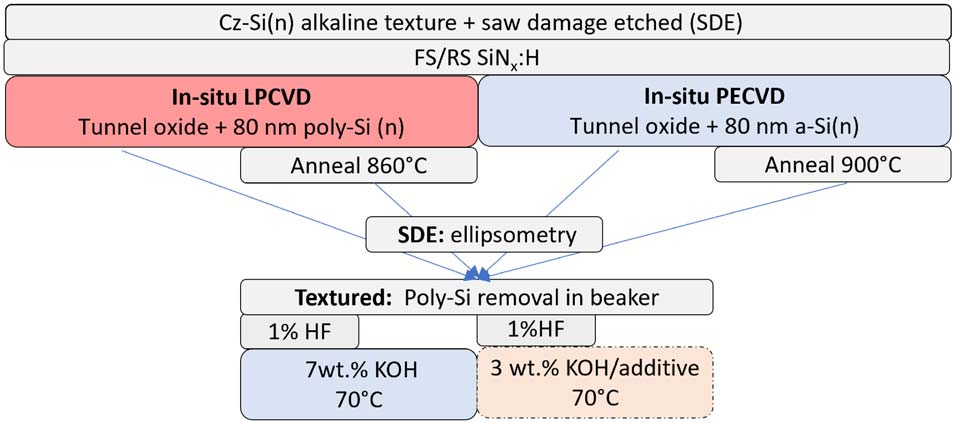
In a pretest we measured layer characteristics of poly-Si and the required time to completely remove the poly-Si layer in heated KOH solution. The n-type Cz-Si test samples, which had been cut from processed wafers, had a size of 20 20 mm2 . The 80 nm thick LPCVD or PECVD poly-Si(n) layer was deposited on top of a 75 nm thick silicon nitride (SiNx, Fig. 3). The poly-Si deposition was carried out in a single run, for both, saw damaged etched and textured samples. The SiNx nitride layer below the poly-Si enhances the visibility of the polysilicon layer removal during etching (similar to Figs. 1a, 1b). SiNx will hardly be etched by KOH and so etching will principally stop there. The temperature for LPCVD deposition was up to 600 °C, for PECVD well below 600 °C. The annealing was performed in nitrogen at 860 °C for LPCVD poly-Si and at 900 °C for PECVD a-Si. Film thickness as well as refractive index n and absorption coefficient k were determined by spectral ellipsometry and evaluated at 632 nm on saw damaged etched wafers (Tab. 1). The higher refractive index of PECVD a-Si is caused by the lower temperature during PECVD deposition, which leads to completely amorphous silicon with a large amount of hydrogen, whereas the higher temperature during LPCVD results in partially crystallized poly-Si with little hydrogen content. After LPCVD annealing, an 8 nm oxide was measured (Tab. 1).

Fig3
3 Results and discussion
Table 2 shows etch rates calculated from measured removal times of 80 nm LPCVD and PECVD TOPCon layers with and without oxide covering the poly-Si. In the presence of an oxide layer on top of a-Si/poly-Si layer the KOH solution with additive ends up with a lower effective etch rate compared to the higher concentrated KOH without additive. Here, the effective etch rate includes the initial low oxide etch rate of the silicon oxide as well as the higher etch rate of poly-Si in KOH. However, if the surface anneal oxide is removed by a HF pre-treatment we see the poly-Si etch rate being equal for both solutions. This finding shows the working principle of the additive which reduces the etch rate for the hydrophilic surface (anneal oxide) and results in an etching selectivity of up to >30:1 for annealed poly-Si (Tab. 2). The etching selectivity is the ratio between the poly-Si etch rate and effective etch rate (initial oxide etch rate and poly-Si etch rate. This effect agrees with poly-Si removal for ex-situ doped poly-Si where an etch rate for n-doped LPCVD poly-Si of 16 nm/s is found and for PSG of 0.1 nm/s in KOH with polish additive, respectively. So, the anneal oxide seems to be sufficiently resistant to retard etching of the poly-Si layer in KOH. In diluted KOH without additive etch rates are reported for n-doped LPCVD poly-Si of 10 nm/s for n-doped PECVD poly-Si of 7 nm/s . Our calculated etch rates might be lower than literature data due to a different additive or experiment design with removal time and the determination of the end point of when etching effectively stops. At the end, sometimes poly-Si residues remained on the wafer as stains in the center of the wafer.
4 Conclusion
The aim of this work was to identify an industrially feasible etch back process sequence with low processing time and uniform etch back quality for the removal of parasitic polySi wrap-around in i-TOPCon solar cells. The poly-Si removal study on wafer level showed that an HF dip prior KOH etching reduces the required KOH etching time by the factor of at least five since the HF removes any oxide on top of the poly-Si and allows for faster attack of the etchant to the poly-Si layer. An additive in the KOH solution enhanced etching of HF treated poly-Si (hydrophobic) and protected the untreated poly-Si/oxide (hydrophilic). Transferred to the solar cell it means that the selective etching between rear and front side in KOH/additive is high enough to realize a batch cluster process for etching annealed poly-Si.