Advent of high mobility perovskite oxide semiconductor BaSnO3 (BSO) has enabled all-perovskite oxide heterostructures such as 2DEGs and FETs. To date all-perovskite oxide device demonstrations have been focused on finding and integrating the compatible perovskite dielectric oxides such as polar LaInO3 and LaScO3 and nonpolar BaHfO3 and SrHfO3. For these demonstrations the length scale of BSO-based heterostructure devices has been about 100 µm, primarily due to the use of stencil masks for patterning. In order to further reduce the length scale, we employed a top-down approach using both photolithography and chemical etching techniques to pattern FETs made entirely of perovskite oxide materials: Ba0.997La0.003SnO3 channel layer, degenerately doped Ba0.96La0.04SnO3 contact layer, and SrHfO3 gate oxide layer. FETs of 3 µm channel length were fabricated using hydrofluoric acid and aqua regia as etchants. The FET exhibits a mobility of 38.8 cm2 /Vs, an on/off ratio of 5.06 × 10⁷ , and a drain current density of 6.05 × 10− 2 mA/μm, consistent with our expectation. These findings demonstrate the feasibility of patterning BSO through photolithography and chemical etching while maintaining the subsequent epitaxial growth, suggesting that BSO can be employed in a broader range of applications as well as for more precise studies of its intrinsic properties.
Introduction
Epitaxial perovskite oxide of ABO3 is the most abundant form of oxides in earth and has been extensively studied for its diverse properties during the last few decades. Recently, BaSnO3 (BSO), a perovskite oxide semiconductor, has been attracting attention as a semiconducting channel material due to the fact that there are many interesting compatible perovskite oxides to be used as gate oxides. Furthermore, it shows the following inherent excellent properties: First, BSO is a cubic perovskite with a lattice constant of 4.116 Å and a wide bandgap semiconductor with a bandgap of 3.1 eV. This means it is suitable for high power devices operating at high voltages. Second, BSO has high mobility. For La-doped BSO (BLSO) single crystals, the high doping region results in high mobility up to 320 cm2 /Vs. Affected by factors such as dislocation, films typically have low mobilities in the range of 20 to 100 cm2 /Vs, but this is comparable or superior to other oxides such as ZnO and SrTiO3 (STO). Third, BSO has high oxygen stability . BSO’s high oxygen stability prevents structural degradation during various manufacturing processes. Fourth, BSO can be easily doped with La . Intrinsically an insulator, BSO can be easily doped with La to degenerate levels, enabling its use as both a channel and contact material. The ability to differentiate the channel and electrode through doping concentrations allows for full perovskite material-based device stacking and low contact resistance between the channel and contact. Due to these characteristics, BSO can produce various FETs by epitaxially depositing other compatible perovskites as gate oxide on the BSO-based metallic contact layer and channel layer with high mobility.
Method
All epitaxial layers used in the FET fabrication were grown using pulsed laser deposition (PLD) at 750 ◦C. BSO and BLSO (Ba1− xLaxSnO3) were deposited under 100 mTorr, while SHO was deposited at 30 mTorr. The laser fluence was uniformly set at 1.43 J/cm2 . The target-sample distance was maintained at 55 mm for BSO and 63 mm for SHO. The targets used for deposition were all produced by Toshima manufacturing Co., Japan. STO substrates were employed, and a 150 nm BSO buffer layer was deposited to minimize the impact of the threading dislocations in BSO coming from the lattice constant mismatch. To define the shapes of the source, drain, channel, and gate electrode, photolithography techniques and wet chemical etching methods were employed. For photolithography, a maskless aligner (Nano system solutions, Inc, DL-1000A1) was utilized. After etching, heated dimethyl sulfoxide (DMSO) at 80 ◦C was used to remove the photoresist.
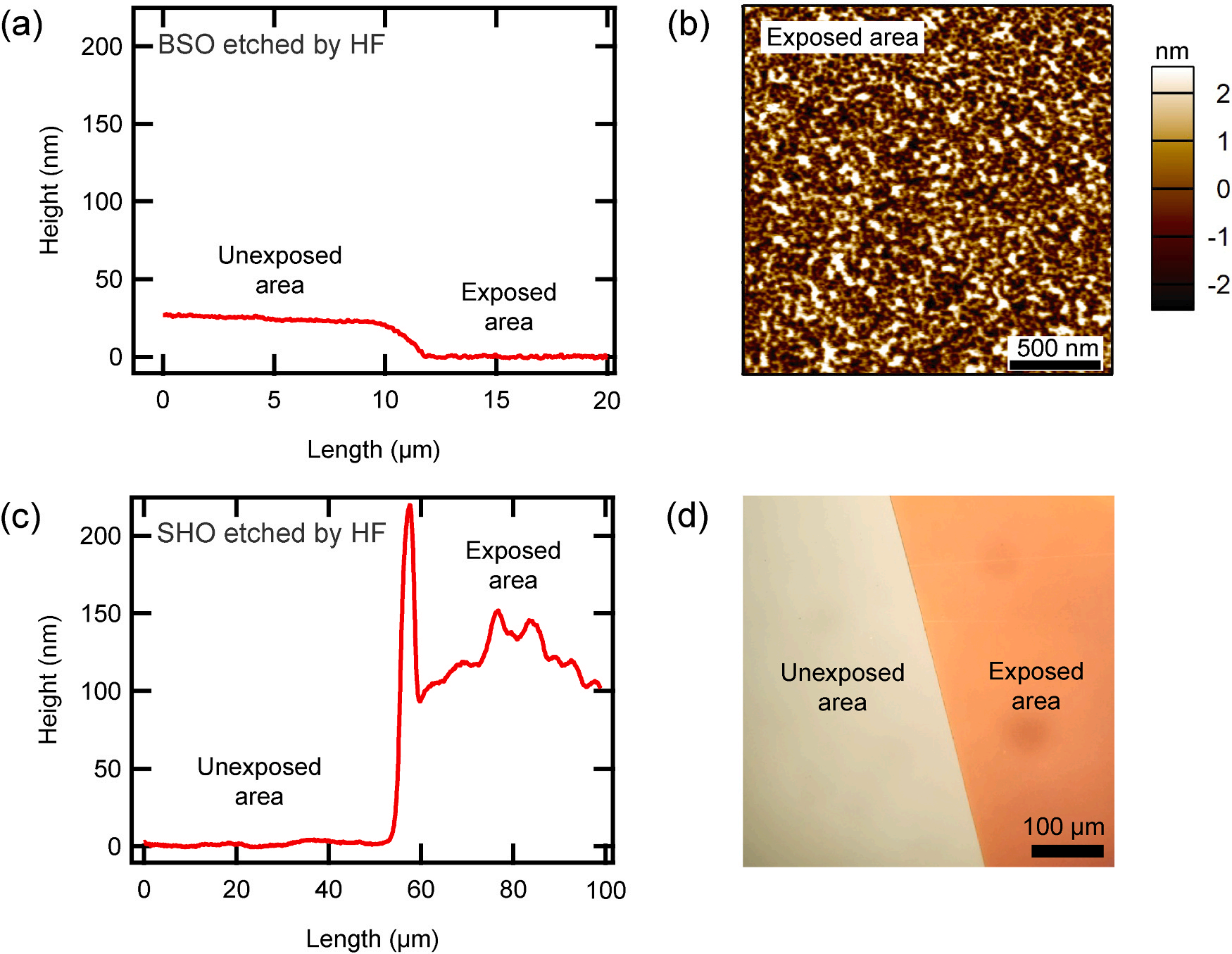
Fig. 1 shows how HF responds to BSO and SHO. Fig. 1a presents the outcome of line profiling, comparing regions of a BSO film that were exposed to HF with those that were not. The exposed area reacted with HF and was etched. To achieve a stable etching rate with hydrofluoric acid, buffered oxide etchant 6:1, a mixture of 40% ammonium fluoride (NH4F) in water and 49% HF in water at a volume ratio of 6:1, was used. This solution was diluted to 1% in distilled water for appropriate etching rates and surface conditions. Etching was performed for 30 s, the etching depth was 23.2 nm, and the etching rate calculated from this was 0.772 nm/s. Fig. 1b is an AFM image of the surface of BSO exposed to HF. The roughness is 1.28 nm, which is almost the same as 1.23 nm before etching. This means that stable etching was achieved. Fig. 1c is the result of line profiling between the exposed and unexposed areas of the SHO film, which was partially exposed to hydrofluoric acid. The etching conditions were the same as for BSO, but the results were completely different from BSO; SHO exposed to hydrofluoric acid showed a higher height than SHO not exposed. Fig. 1d is an optical microscope image of SHO film partially etched with hydrofluoric acid. It was confirmed that a clear boundary was created due to etching. These mean that the product formed by the reaction between SHO and hydrofluoric acid does not dissolve in water and remains on the film surface in the form of a salt. The generated salt remains on the film and has a higher height than the unexposed portion. Hafnium combines with fluorine to form HfF4 (Hf + 2 F2 → HfF4 (s)), which is insoluble in water, so the salt is assumed to be HfF4. If the salt was on the film surface, it would easily come off physically, so we wiped the entire film using a cotton swab to confirm. After wiping, it was confirmed through an optical microscope image that some of the salt could be wiped off.

Fig. 1. Etching by HF. (a) and (c) are the depth profiling between exposed and unexposed areas when parts of BSO and SHO films were exposed to HF, respectively. In both cases, the etching time is 30 s and 1/100 diluted buffered oxide etchant was used. (b) is an AFM image of the surface of BSO exposed to HF. (d) is an optical microscopy image of a SHO film partially exposed to HF.
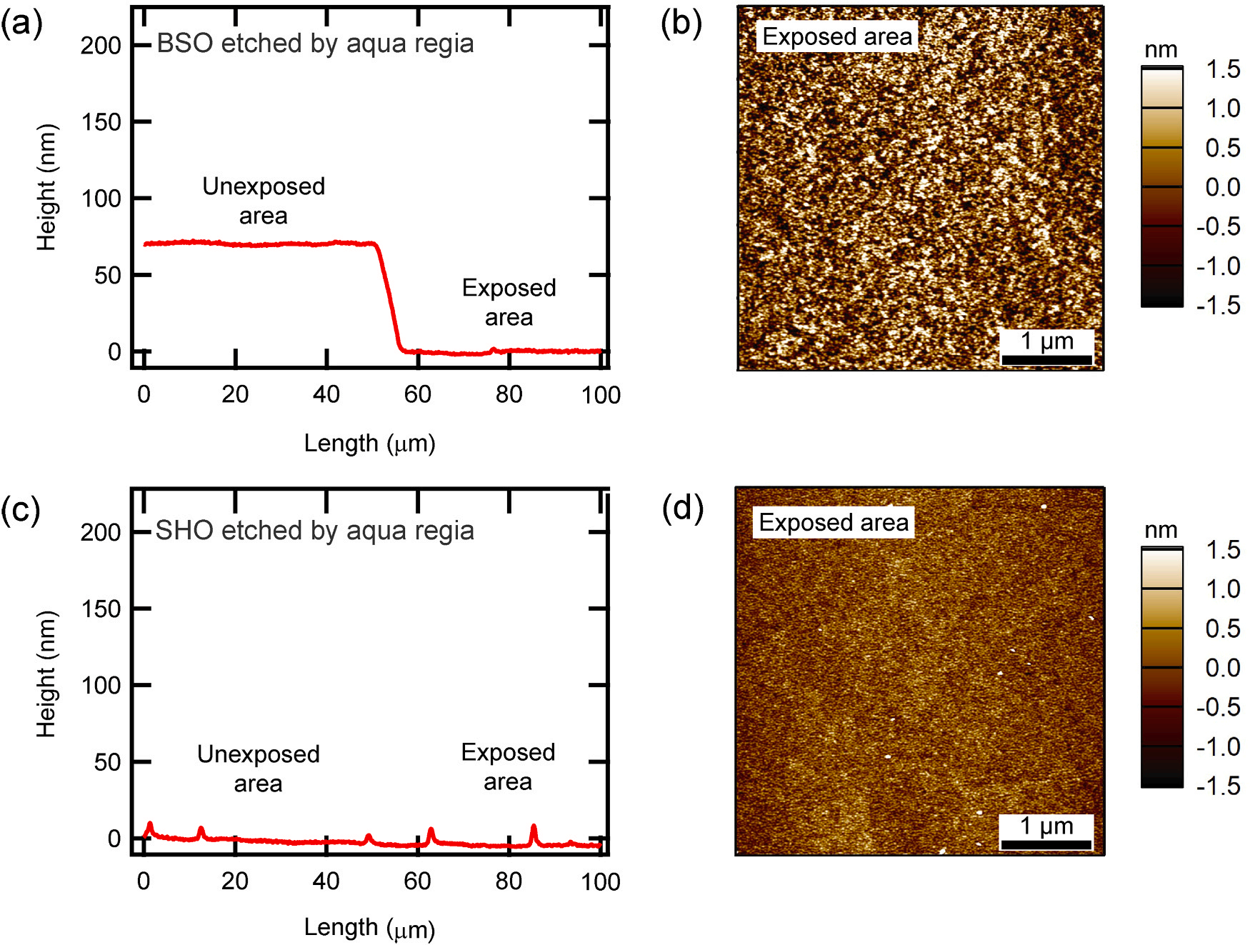
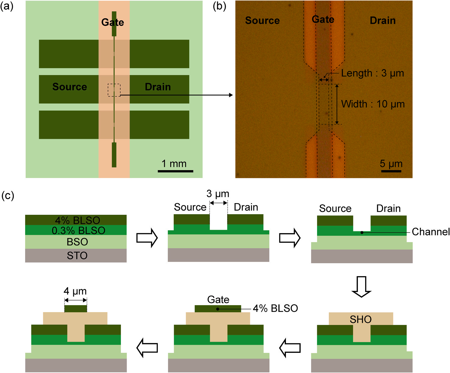
Fig. 2 shows how aqua regia reacts to BSO and SHO. Fig. 2a depicts the line profile comparison of a BSO film, showing differences between areas exposed to aqua regia and those that were not. As in the case of hydrofluoric acid, BSO was also etched by aqua regia. Aqua regia was prepared by mixing 35% HCl and 60% HNO3 in a volume ratio of 3:1 immediately before etching. And to control the etching rate, it was diluted to 1/4 with distilled water. Etching was performed for 60 s, the etching depth was 70.5 nm, and the etching rate was 1.175 nm/s. However, the etching rate of aqua regia showed a large variation, ranging from 0.079 to 1.53 nm/s, even when aqua regia was produced using the same recipe. This is thought to be because the reaction of aqua regia itself varies greatly over time. Due to the etching rate that changes in time, aqua regia is not suitable for etching that requires precise depth control. However, it can be used when etching the entire thickness of the BSO film. Fig. 2b is an AFM image of the surface of BSO etched with aqua regia. The roughness is 868 pm, showing a flat surface. On the other hand Fig. 2c shows the line profiling results for a SHO film, contrasting the sections exposed to aqua regia with the unexposed areas. Although the etching conditions are the same as for BSO, unlike BSO, SHO exposed to aqua regia did not change height, meaning that SHO does not react with aqua regia. Fig. 2d is an AFM image of the surface of SHO exposed to aqua regia. The roughness shows a low value of 310 pm. The fact that SHO is not etched by aqua regia could be an advantage in fabrication. Especially in situations where it is difficult to etch BSO with aqua regia to the exact desired thickness, SHO can be used as an etching stop layer. In addition, the XRD data of the FET in Fig. S1 suggest that epitaxial growth can be maintained on the etched surfaces. Fig. 3 shows the shape and fabrication process of the FET using chemical etching. Fig. 3a presents the schematic top view of the entire device.

Fig. 2. Etching by aqua regia. (a) and (c) are the depth profiling between exposed and unexposed areas when parts of BSO and SHO films were exposed to aqua regia, respectively. In both cases, the etching time is 60 s and 1/4 diluted aqua regia was used. (b) and (d) are AFM images of the surface of BSO and SHO exposed to aqua regia, respectively.

Fig. 3. FET fabricated using chemical etching. (a) Schematic top view of the FET. (b) Optical microscope image of the FET. (c) Schematic fabrication process of FET. 4% BLSO for source-drain, 0.3% BLSO for channel and BSO for buffer are deposited in-situ. Source, drain, and channel structure is fabricated using HF. Gate electrode is patterned using aqua regia.
Fig. 3b is the optical microscope view of the device’s source, drain, and gate structure. Fig. 3c is the fabrication process of FET using chemical etching on an STO substrate. A BSO buffer layer of 150 nm is first deposited to reduce the dislocation density, followed in situ by a 20 nm layer of 0.3% BLSO for the channel and a 55 nm layer of 4% BLSO for the contact layer. Subsequently, HF is used to etch 55 nm, exposing the 0.3% BLSO layer, except where the source and drain pads will be formed. The gap between these pads, set at 3 µm, defines the channel length. Another etching step with HF is then performed to expose the BSO buffer layer up to 24 nm, except for the areas designated for the channel and contact pads. These two etching steps result in a source, drain, and channel structure with a channel length of 3 µm and a width of 10 µm. Next, using a stencil mask and PLD, SHO is deposited as the gate oxide to a thickness of 197 nm, followed by a 50 nm layer of 4% BLSO for the electrode. The gate oxide and electrode widths are set at 860 µm and 120 µm, respectively. To reduce leakage current by minimizing the overlap between the source, drain, and gate electrode, an etching process is conducted to reduce the width of the gate electrode to 4 µm, using aqua regia. During this process, SHO acts as an etching stop layer for the aqua regia.
Results and discussion
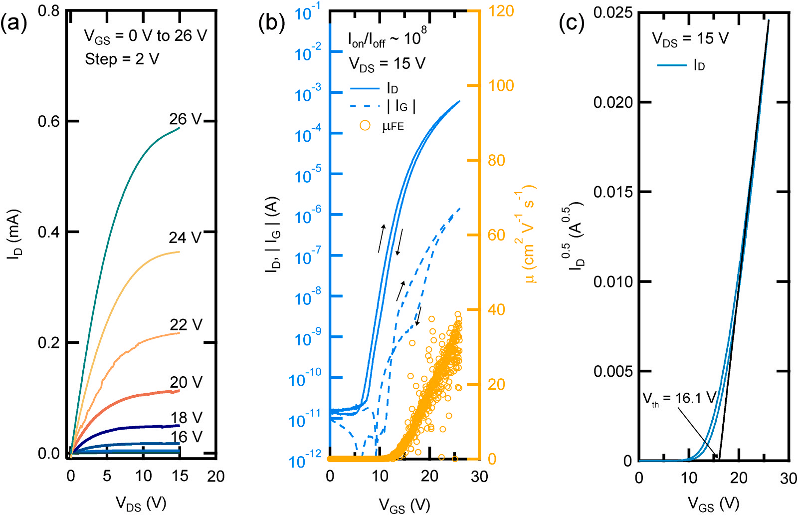
We have measured the electrical characteristics of our fully epitaxial FET. Fig. 4a shows the output characteristics of our device, with drain voltage (VDS) measured from 0 to 15 V, and gate voltage (VGS) sequentially measured from 0 to 26 V in 2 V intervals. An increase in the drain current was observed as both VDS and VGS increased, and saturation of the drain current at high drain voltages was noted. It can be observed that the voltage at which the drain current saturates does not significantly differ from that of previous FETs with larger lengths. There are two factors that determine the saturation of the drain current. These are pinch-off and electron velocity saturation. The drain current saturated by pinch-off is proportional to the square of VGS, and the drain current saturated by the saturation velocity of electrons is proportional to VGS. Based on this, we can see that the saturation of the drain current of our device is caused by pinch-off. Fig. 4b displays the transfer characteristics, where VGS was swept from − 3 to 26 V while VDS was held at the saturation region of 15 V. From this transfer curve, the field effect mobility was calculated. The maximum mobility was measured at 38.8 cm2 /Vs. The drain current density increased up to 6.05 × 10− 2 mA/μm when VGS was at 26 V. The ratio of the highest to the lowest drain current is 5.06 × 10⁷, and the subthreshold swing is 0.93 V /dec. The subthreshold swing was calculated from the equation S = [∂ log₁₀ (IDS)/∂VGS]⁻ 1 . The threshold voltage (Vth) of our device is 16.1 V, obtained from a graph plotting ID 0.5 vs. VGS (Fig. 4c).

Fig. 4. Electrical characteristics of FET. (a) Output and (b) transfer characteristic of the FET. (c) Square root of drain current as a function of gate voltage in saturation region. Using extrapolation, we obtained a threshold voltage of 16.1 V.
Conclusion
In summary, we have successfully fabricated a micron-scale, fully epitaxial accumulation-mode BSO-based FET with a channel length of 3 µm using photolithography and chemical etching. In the saturation region, the drain current density reached up to 6.05 × 10− 2 mA/μm. This is lower compared to submicron scale FETs but higher than those reported for fully epitaxial BSO-based FETs with a longer channel length. When compared to previously reported SHO FETs, the scaling of the drain current density seems reasonable. The mobility was measured at 38.8 cm2 /Vs, which is lower than that of previous all-epitaxial BSObased FETs. We believe further optimization of surface treatment will lead to improvements in mobility. Our work demonstrates the feasibility of fabricating smaller-sized epitaxial devices using accessible and straightforward wet etching methods for BSO. Going forward, this approach is expected to enable easy fabrication of various heterostructures and to facilitate detailed studies into the intrinsic properties of BSO.